Categories: Featured Articles » Practical Electronics
Number of views: 13954
Comments on the article: 1
Choosing a driver for MOSFET (example calculation by parameters)
FET gate control is an important aspect in the development of any modern electronic device. For example, when only the lower power switch is used in a pulse converter, and the decision is made in favor of using an individual driver in the form of a specialized microcircuit, it is necessary to solve the problem of selecting a suitable driver so that it can satisfy the following conditions.
First, the driver will need to provide reliable opening and closing of the selected key. Secondly, it is necessary to comply with the requirements for an adequate duration of the leading and trailing edges during switching. Thirdly, the driver itself should not be overloaded while working in the circuit.
At this stage, it is advisable to start by analyzing the data from the documentation for the field effect transistor, and from these to determine what the characteristics of the driver should be. After that, it remains to choose a specific driver chip from those offered on the market.
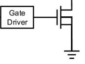
The amplitude of the control voltage is 12 volts
In the datasheet on the field effect transistor there is a parameter Vgs (th) - this is the minimum voltage between the gate and the source at which the transistor will already begin to open quietly. Usually its value is within 4 volts.
Further, when the voltage at the gate rises to about 6 volts, a phenomenon such as the “Miller plateau” will surely manifest itself, consisting in the fact that during the opening of the transistor, due to the induced influence of the incident voltage on the drain, the gate-source capacitance is temporarily as if will increase, and although the shutter will continue to receive charge from the driver, the voltage on it relative to the source will not increase further for some time.
However, after overcoming the Miller plateau, the gate voltage will continue to increase linearly, and the drain current will linearly reach its maximum in time for the moment when the gate voltage is about 7-8 volts.

Since the charging process of any capacity proceeds exponentially, that is, at the end it always slows down, then for a faster shutter charge, so as not to delay the process of opening the transistor, the output voltage of the driver Uupr is taken to be 12 volts. Then 7-8 volts - this will be just 63% of the amplitude, to which the voltage will grow almost linearly for a time equal to 3 * R * Ciss, where Ciss is the current gate capacitance, and R is the resistance in the gate-source section.
Full Gate Charge Qg
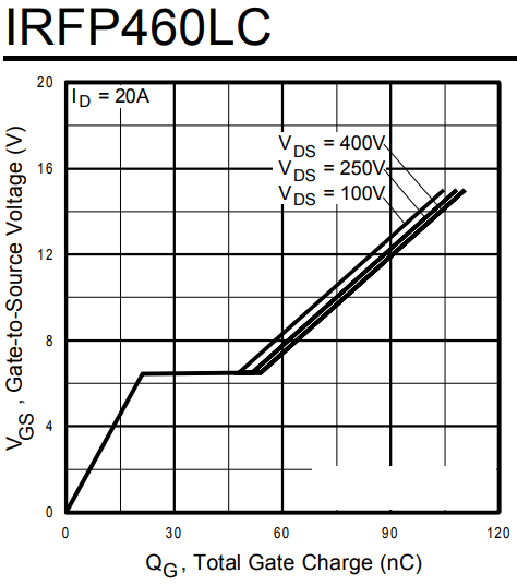
When the driver voltage is selected, the total gate charge Qg is taken into account. This is a place of compromise between the peak current of the Imax driver and the opening time of the transistor Tvcl. First, they recognize the full gate charge Qg, which the driver will have to transfer to the gate at the beginning of each key operating cycle, and at the end of each cycle, remove it from the shutter.
We will find the full shutter charge according to the graph from the datasheet, where depending on the voltage that was originally assumed to be on the drain, Qg at 12 volts Uupr will be different.
How long the shutter should be fully charged - this actually depends either on how long it takes to get the front of the power transistor to open, or on which driver is available. The driver you select must have the appropriate Rise Time and Fall Time options.
But since we decided that we would choose the driver based primarily on the needs of the developed circuit, we will begin the calculation precisely from the time during which the transistor will have to fully open (or close). We divide the gate charge Qg by the value of the required time for opening (or closing) the key T on (off) - we obtain the average current coming out of the driver passing through the gate:
Iav = Qg / Tincl.
Peak current driver Imax
Since, as a whole, the shutter charge process proceeds almost uniformly, we can assume that the driver’s output current will drop to almost zero by the time the shutter is fully charged (to the voltage Uupr). Therefore, we assume that the peak driver current Imax is equal to twice the average current value: Imax = Iav * 2, then the driver will definitely not burn out from overload on the output current. As a result, we select the driver based on Imax and Upr.
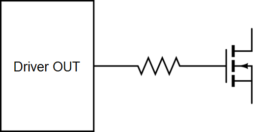
If the driver is already at our disposal, and Imax is more than the peak current of the driver. We simply divide the amplitude of the control voltage Uupr by the value of the maximum current Imax driver.
According to Ohm's law, we get the value of the minimum resistance that you need to have in the gate circuit in order to limit the gate charge current to the peak current declared in the datasheet for the existing driver:
Rgate = Upr / Imax driver
In the datasheet, the value Rg is sometimes indicated - the resistance of the gate-source section. It is important to take it into account, and if this value is enough, then an external resistor is not necessary. If you need to further limit the current, you will also have to add an external resistor. When an external resistor is added, this will affect the key opening time.
The increased parameter R * Ciss should not lead to exceeding the desired duration of the leading edge, therefore, this parameter must be calculated.
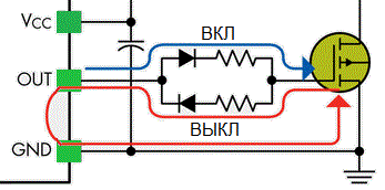
As for the process of locking the key, here the calculations are carried out similarly. If, however, it is necessary that the durations of the leading and trailing edges of the control pulses differ from each other, then it is possible to put separate RD-chains on the charge and on the shutter discharge in order to obtain different time constants for the beginning and for the completion of each working cycle. Again, it is important to remember that the selected driver will have to have the appropriate minimum Rise Time and Fall Time parameters, which must be less than the required ones.
See also at i.electricianexp.com
:
