Categories: Featured Articles » Practical Electronics
Number of views: 30915
Comments on the article: 1
RCD snubber - principle of operation and calculation example
The reason they resort to the use of snubbers
During the development of a power pulse converter (especially for powerful push-pull and forward topology devices, where switching occurs in hard modes), care must be taken to protect the power switches from voltage breakdown.
Despite the fact that the fieldwork documentation indicates the maximum voltage between the drain and source at 450, 600 or even 1200 volts, one random high-voltage pulse on the drain may be enough to break the expensive (even high-voltage) key. Moreover, neighboring elements of the circuit, including a scarce driver, may come under attack.
Such an event will immediately lead to a bunch of problems: where to get a similar transistor? Is it on sale now? If not, when will it appear? How good will the new fieldwork be? Who, when and for what money will undertake to solder all this? How long will the new key last and will it not repeat the fate of its predecessor? etc.
In any case, it is better to be safe at once, and even at the design stage of the device take measures to prevent such troubles at the root. Fortunately, a reliable, inexpensive and easy-to-implement solution based on passive components has been known for a long time that has become popular among both fans of high-voltage power equipment and professionals. It's about the simplest RCD snubber.

Traditionally for pulse converters, the inductance of the primary winding of a transformer or inductor is included in the drain circuit of a transistor. And with a sharp shutdown of the transistor under conditions when the switched current has not yet decreased to a safe value, according to the law of electromagnetic induction, a high voltage will appear on the winding, proportional to the inductance of the winding and the transition speed of the transistor from the conducting state to the locked state.
If the front is steep enough, and the total inductance of the winding in the drain circuit of the transistor is significant, then the high rate of voltage rise between the drain and the source will instantly lead to disaster. In order to reduce and facilitate this thermal growth rate of locking the transistor, an RCD snubber is placed between the drain and the source of the protected key.
How does the RCD snubber work?

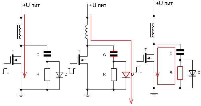
RCD snabber works as follows. At the moment the transistor is locked, the current of the primary winding, due to its inductance, cannot instantly decrease to zero. And instead of burning the transistor, the charge, under the action of high EMF, rushes through the diode D to the capacitor C of the snubber circuit, charging it, and the transistor closes in the soft mode of a small current through its transition.
When the transistor starts to open again (abruptly transitioning to the next switching period), the snubber capacitor will discharge, not through the bare transistor, but through the snubber resistor R. And since the snubber resistor is several times greater than the drain transition resistance source, then the main part of the energy stored in the capacitor will be allocated exactly on the resistor, and not on the transistor. Thus, the RCD snubber absorbs and dissipates the energy of the spurious high-voltage surge c inductance.
Snubber chain calculation

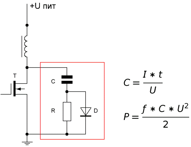
P - power dissipated on the snubber resistor C - snubber capacitor capacity t - transistor locking time, during which the snubber capacitor is charged U - the maximum voltage to which the snubber capacitor is charged I - the current through the transistor until it closes f- how many times per second snabber (transistor switching frequency)
To calculate the values of the protective snubber elements, for a start, they are set by the time for which the transistor in this circuit goes from the conducting state to the locked state. During this time, the snubber capacitor must have time to charge through the diode. Here, the average current of the power winding is taken into account, from which it is necessary to protect. And the supply voltage of the converter winding will allow you to choose a capacitor with a suitable maximum voltage.
Next, you need to calculate the power that will be dissipated by the snubber resistor, and after that select the specific value of the resistor based on the time parameters of the obtained RC circuit. Moreover, the resistance of the resistor should not be too small, so that when the capacitor starts to discharge through it, the pulse of the maximum discharge current together with the operating current does not exceed the critical value for the transistor. This resistance should not be too large so that the capacitor still has time to discharge, while the transistor is working out the positive part of the working period.
Let's look at an example.
A network push-pull inverter (amplitude of a supply voltage of 310 volts) consuming 2 kW operates at a frequency of 40 kHz, and the maximum voltage between the drain and the source for its keys is 600 volts. It is necessary to calculate the RCD snubber for these transistors. Let the turn-off time of the transistor in the circuit be 120 ns.
The average winding current 2000/310 = 6.45 A. Let the voltage on the key not exceed 400 volts. Then C = 6.45 * 0.000000120 / 400 = 1.935 nF. We choose a film capacitor with a capacity of 2.2 nF at 630 volts. The power absorbed and dissipated by each snubber for 40,000 periods will be P = 40,000 * 0.0000000022 * 400 * 400/2 = 7.04 W.
Suppose the minimum pulse duty cycle on each of the two transistors is 30%. This means that the minimum open time of each transistor will be 0.3 / 80,000 = 3.75 μs, taking into account the front, we take 3.65 μs. We take 5% of this time for 3 * RC, and let the capacitor have almost completely discharged during this time. Then 3 * RC = 0.05 * 0.00000365. From here (substitute C = 2.2 nF) we get R = 27.65 Ohms.
We install two five-watt resistors of 56 Ohms in parallel in each snubber of our two-stroke, and we get 28 Ohms for each snubber. The pulse current from the operation of the snubber when the capacitor discharges through the resistance is 400/28 = 14.28 A - this is the current in the pulse that passes through the transistor at the beginning of each period. According to the documentation for most popular power transistors, the maximum allowable pulse current for them exceeds the maximum average current by at least 4 times.
As for the diode, a pulse diode is placed in the RCD snubber circuit at the same maximum voltage as that of the transistor, and is able to withstand the maximum current flowing through the primary circuit of this converter in a pulse.
See also at i.electricianexp.com
:
