Categories: Featured Articles » Novice electricians
Number of views: 108661
Comments on the article: 3
The device and operation of the bipolar transistor
 A transistor is an active semiconductor device, with the help of which amplification, conversion and generation of electrical oscillations is carried out. Such an application of the transistor can be observed in analogue technology. Besides transistors They are also used in digital technology, where they are used in key mode. But in digital equipment, almost all transistors are “hidden” inside integrated circuits, and in huge quantities and in microscopic sizes.
Here we will not dwell too much on the electrons, holes, and atoms, which were already described in the previous parts of the article, but some of this, if necessary, will still have to be remembered.
The semiconductor diode consists of one p-n junction, the properties of which were described in the previous part of the article. The transistor, as you know, consists of two transitions, therefore semiconductor diode can be considered as the precursor of the transistor, or its half.
If the p-n junction is at rest, then the holes and electrons are distributed, as shown in Figure 1, forming a potential barrier. We will try not to forget the conventions of electrons, holes, and ions shown in this figure.

Picture 1.
How is a bipolar transistor
Device bipolar transistor simple at first glance. To do this, it is enough to create two pn junctions on one semiconductor wafer, called the base. Some methods for creating a pn junction have been described. in previous parts of the articletherefore we will not repeat here.
If the base conductivity is of type p, then the resulting transistor will have the structure n-p-n (pronounced "en-pe-en"). And when an n-type plate is used as the base, then we get a transistor of the p-n-p structure (pe-en-pe).
As soon as it came to the base, you should pay attention to this thing: the semiconductor wafer used as the base is very thin, much thinner than the emitter and collector. This statement should be remembered, because it will be needed in the process of explaining the operation of the transistor.
Naturally, to connect to the "outside world" from each region p and n comes wire output. Each of them has the name of the area to which it is connected: emitter, base, collector. Such a transistor is called a bipolar transistor, because it uses two types of charge carriers - holes and electrons. The schematic structure of transistors of both types is shown in Figure 2.
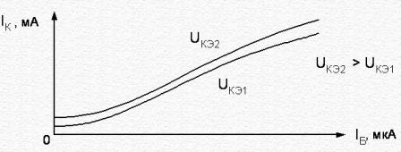
Figure 2
Currently, silicon transistors are used to a greater extent. Germanium transistors are almost completely obsolete, being supplanted by silicon, so the further story will be about them, although germanium will sometimes be mentioned. Most silicon transistors have an n-p-n structure, since this structure is more technologically advanced in production.
Complementary pairs of transistors
For germanium transistors, apparently, the p-n-p structure was more technologically advanced, so germanium transistors for the most part had precisely this structure. Although, as part of complementary pairs (transistors close in parameters, which differed only in the type of conductivity), germanium transistors of different conductivity were also produced, for example, GT402 (p-n-p) and GT404 (n-p-n).
Such a pair was used as output transistors in ULF of various radio equipment. And if non-modern germanium transistors have gone down in history, then complementary pairs of silicon transistors are still being produced, starting from transistors in SMD-packages and up to powerful transistors for output stages of ULF.
By the way, sound amplifiers on germanium transistors were perceived by music lovers almost like tube ones. Well, maybe a little worse, but much better than silicon transistor amplifiers. This is just for reference.
How does a transistor work
In order to understand how the transistor works, we will again have to return to the world of electrons, holes, donors and acceptors. True, now it will be somewhat simpler, and even more interesting than in the previous parts of the article. Such a remark had to be made in order not to frighten the reader, to allow to read all this to the end.
Figure 3 above shows the conditional graphic designation of transistors on electrical circuits, and below p-n junctions of transistors are presented in the form of semiconductor diodes, which are also included in the opposite direction. This representation is very convenient when checking the transistor with a multimeter.
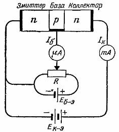
Figure 3
And figure 4 shows the internal structure of the transistor.
In this figure, you have to linger a bit to consider it in more detail.
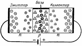
Figure 4
So will the current pass or not?
Here it is shown how the power source is connected to the transistor of the n-p-n structure, and it is in such a polarity that it is connected to real transistors in real devices. But, if you look closely, it turns out that through two p-n junctions, through two potential barriers, the current will not pass: no matter how you change the polarity of the voltage, one of the junctions will necessarily be in a locked, non-conducting state. So for now let’s leave everything as shown in the figure and see what happens there.
Uncontrolled current
When you turn on the current source, as shown in the figure, the emitter-base (n-p) transition is in the open state and will easily let the electrons pass from left to right. After which the electrons will collide with a closed junction base emitter (p-n), which will stop this movement, the path for electrons will be closed.
But, as always and everywhere, there are exceptions to all rules: some very nimble electrons will be able to overcome this barrier under the influence of temperature. Therefore, although an insignificant current with such an inclusion will still be. This minor current is called the initial current or saturation current. The last name is due to the fact that all free electrons that are capable of overcoming the potential barrier at a given temperature participate in the formation of this current.
The initial current is uncontrollable, it is available for any transistor, but at the same time it is little dependent on external voltage. If it, the voltage, is increased significantly (within the reasonable range indicated in the directories), the initial current will not change much. But the thermal effect on this current is very noticeable.
A further increase in temperature causes an increase in the initial current, which in turn can lead to additional heating of the pn junction. Such thermal instability can lead to thermal breakdown, destruction of the transistor. Therefore, measures should be taken to cool the transistors, and do not apply extreme stresses at elevated temperatures.
Now remember the base
The inclusion of a dangling-base transistor described above is not applied anywhere in practical schemes. Therefore, Figure 5 shows the correct inclusion of the transistor. To do this, it was necessary to apply some small voltage to the base relative to the emitter, and in the forward direction (recall the diode, and look again at Figure 3).
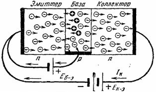
Figure 5
If in the case of the diode, everything seems to be clear, - the current opened and went through it, then other events occur in the transistor. Under the action of the emitter current, the electrons rush to the base with conductivity p from the emitter with conductivity n. In this case, part of the electrons will be filled by holes located in the base region and an insignificant current flows through the base terminal - the base current Ib. This is where it should be remembered that the base is thin and there are few holes in it.
The remaining electrons, which did not have enough holes in the thin base, rush into the collector and will be extracted from there by the higher potential of the Ek-e collector battery. Under this influence, the electrons overcome the second potential barrier and return to the emitter through the battery.
Thus, a small voltage applied to the base - emitter junction helps open the base - collector junction, which is biased in the opposite direction. Actually, this is the transistor effect.
It remains only to consider how this "small voltage" applied to the base affects the collector current, what are their values and ratios. But about this story in the next part of the article about transistors.
Continuation of the article: Characteristics of Bipolar Transistors
Boris Aladyshkin
See also at i.electricianexp.com
: