Categories: Featured Articles » Practical Electronics
Number of views: 30266
Comments on the article: 0
Bipolar transistors: circuits, modes, modeling
The transistor appeared in 1948 (1947), thanks to the work of three engineers and Shockley, Bradstein, Bardin. In those days, their rapid development and popularization were not yet anticipated. In the Soviet Union in 1949, the prototype of the transistor was presented to the scientific world by the Krasilov laboratory, it was the C1-C4 triode (germanium). The term transistor appeared later, in the 50s or 60s.
However, they found widespread use in the late 60s and early 70s, when portable radios came into fashion. By the way, they have long been called the "transistor". This name stuck due to the fact that they replaced electronic tubes with semiconductor elements, which caused a revolution in radio engineering.
What is a semiconductor?
Transistors are made of semiconductor materials, for example, silicon, germanium was previously popular, but now it is rarely found, due to its high cost and worse parameters, in terms of temperature and other things.
Semiconductors are materials that occupy a place between conductors and dielectrics in conductivity. Their resistance is a million times greater than conductors, and hundreds of millions of times less than dielectrics. In addition, in order for the current to flow through them, it is necessary to apply a voltage exceeding the band gap so that the charge carriers pass from the valence band to the conduction band.
The conductors of the forbidden zone are not present as such. A charge carrier (electron) can move into the conduction band not only under the influence of external voltage, but also from heat - this is called thermal current. The current caused by the irradiation of the light flux of the semiconductor is called the photocurrent. Photoresistors, photodiodes and other photosensitive elements work on this principle.
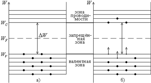
For comparison, look at those in dielectrics and conductors:
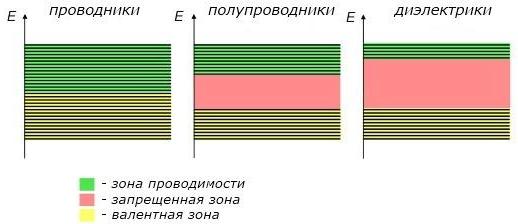
Pretty obvious. The diagrams show that dielectrics can still conduct current, but this happens after overcoming the forbidden zone. In practice, this is called dielectric breakdown voltage.
So, the difference between germanium and silicon structures is that for germanium the band gap is of the order of 0.3 eV (electron volts), and that of silicon is more than 0.6 eV. On the one hand, this causes more losses, but the use of silicon is due to technological and economic factors.
As a result of doping, a semiconductor receives additional charge carriers positive (holes) or negative (electrons), this is called a p- or n-type semiconductor. You may have heard the phrase “pn junction.” So this is the boundary between semiconductors of different types. As a result of the movement of charges, the formation of ionized particles of each type of impurity to the main semiconductor, a potential barrier forms, it does not allow the current to flow in both directions, more about this is described in the book "The transistor is easy.".
The introduction of additional charge carriers (doping of semiconductors) made it possible to create semiconductor devices: diodes, transistors, thyristors, etc. The simplest example is a diode, the operation of which we examined in the previous article.
If you apply a voltage in a forward bias, i.e. I’ll flow positive to the p-region, and a negative current will flow to the n-region, and if the opposite is true, the current will not flow. The fact is that with direct bias, the main carriers of the p-region (hole) are positive, and repel from the positive potential of the power source, tend to the region with a more negative potential.
At the same time, negative carriers of the n-region repel from the negative pole of the power source. Both carriers tend to the interface (pn junction).The transition becomes narrower, and carriers overcome the potential barrier, moving in areas with opposite charges, where they recombine with them ...
If a reverse bias voltage is applied, then the positive carriers of the p-region move toward the negative electrode of the power source, and the electrons from the n-region move toward the positive electrode. The transition expands, the current does not flow.
If you do not go into details, this is enough to understand the processes taking place in a semiconductor.
Conditional graphic designation of the transistor
In the Russian Federation, such a transistor designation is adopted as you see in the picture below. The collector is without an arrow, the emitter is with an arrow, and the base is perpendicular to the line between the emitter and the collector. The arrow on the emitter indicates the direction of current flow (from plus to minus). For the NPN structure, the emitter arrow is directed from the base, and for the PNP, it is directed to the base.
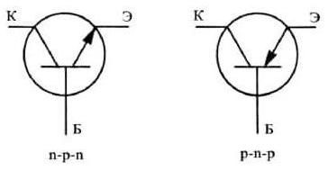
Moreover, the same designation is often found in schemes, but without a circle. The standard letter designation is “VT” and the number in order on the diagram, sometimes they simply write “T”.
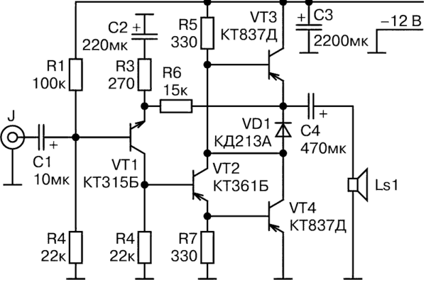
Image of transistors without a circle
What is a transistor?
A transistor is an active semiconductor device designed to amplify a signal and generate oscillations. He replaced the vacuum tubes - triodes. Transistors usually have three legs - a collector, emitter and base. The base is the control electrode, supplying current to it, we control the collector current. Thus, with the help of a small base current, we regulate large currents in the power circuit, and the signal is amplified.
Bipolar transistors are direct forward (PNP) and reverse conductivity (NPN). Their structure is depicted below. Typically, the base occupies a smaller volume of the semiconductor crystal.

Specifications
The main characteristics of bipolar transistors:
-
Ic - maximum collector current (cannot be higher - it will burn);
-
Ucemax - maximum voltage that can be applied between the collector and the emitter (it is impossible to above - it will break);
-
Ucesat is the saturation voltage of the transistor. Voltage drop in saturation mode (the smaller, the less losses in the open state and heating);
-
Β or H21E - gain of the transistor, equal to Ik / Ib. Depends on the transistor model. For example, at a gain of 100, at a current through the base of 1 mA, a current of 100 mA will flow through the collector, etc.
It is worth saying about the transistor currents, there are three of them:
1. The base current.
2. Collector current.
3. Emitter current - contains the base current and emitter current.
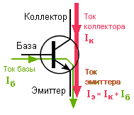
Most often, the emitter current drops because it almost does not differ from the collector current in magnitude. The only difference is that the collector current is less than the emitter current by the value of the base current, and since transistors have a high gain (say 100), then at a current of 1A through the emitter, 10mA will flow through the base, and 990mA through the collector. Agree, this is a small enough difference to spend time on it when studying electronics. Therefore, in the characteristics and indicated Icmax.
Operating modes
The transistor can work in different modes:
1. Saturation mode. In simple words, this is the mode in which the transistor is in the maximum open state (both transitions are biased in the forward direction).
2. The cutoff mode is when the current does not flow and the transistor is closed (both transitions are biased in the opposite direction).
3. Active mode (collector-base is biased in the opposite direction, and the emitter-base is biased in the forward direction).
4. Inverse active mode (collector-base is biased in the forward direction, and the emitter-base is biased in the opposite direction), but it is rarely used.
Typical transistor switching circuits
There are three typical transistor switching circuits:
1. The general base.
2. General emitter.
3. The common collector.

The input circuit is considered to be the emitter base, and the output circuit is the collector-emitter. Whereas the input current is the base current, and the output is the collector current, respectively.
Depending on the switching circuit, we amplify the current or voltage.In textbooks, it is customary to consider just such inclusion schemes, but in practice they do not look so obvious.
It is worth noting that when connected to a circuit with a common collector, we amplify the current and get in-phase (the same as the input in polarity) voltage at the input and output, and in the circuit with a common emitter, we get the voltage and inverse voltage gain (the output is inverted relative to input). At the end of the article, we will simulate such circuits and clearly see this.
Transistor Key Modeling
The first model we will look at is key mode transistor. To do this, you need to build a circuit as in the figure below. Suppose that we will include a load with a current of 0.1A, its role will be played by the resistor R3 installed in the collector circuit.
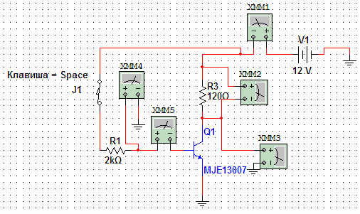
As a result of experiments, I found that the h21E of the selected transistor model is about 20, by the way, in the datasheet on MJE13007 it says from 8 to 40.

Base current should be around 5mA. The divider is calculated so that the base current has a minimal effect on the divider current. So that the specified voltage does not float when the transistor is turned on. Therefore, the current divider set 100mA.
Rbrosch = (12V - 0.6v) /0.005= 2280 Ohm
This is a calculated value, the currents as a result of this came out as follows:
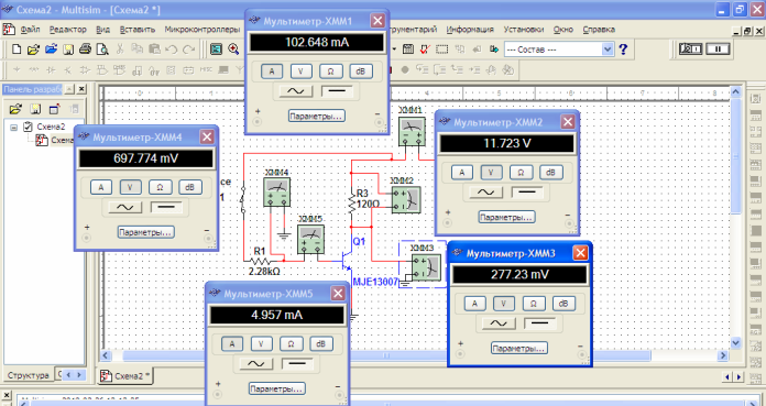
With a base current of 5mA, the current in the load was about 100mA, the voltage drops to 0.27V at the transistor. The calculations are correct.
What did we get?
We can control a load whose current is 20 times the control current. To further amplify, you can duplicate the cascade, reducing the control current. Or use another transistor.
The collector current was limited by the load resistance, for the experiment I decided to make the load resistance 0 Ohm, then the current through the transistor is set by the base current and gain. As a result, the currents practically do not differ, as you can see.
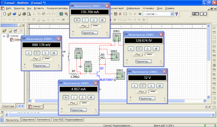
To trace the effect of the type of transistor and its gain on currents, we replace it without changing the circuit parameters.
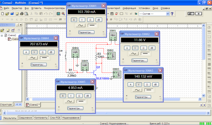
After replacing the transistor from MJE13007 to MJE18006, the circuit continued to work, but 0.14 V drops on the transistor, which means that at the same current this transistor will heat up less, because will stand out in heat
Pot = 0.14V * 0.1A = 0.014W,
And in the previous case:
Potprevious = 0.27V * 0.1A = 0.027W
The difference is almost twofold, if it is not so significant at tenths of watts, imagine what will happen at currents of tens of amperes, then the power of losses will increase 100 times. This leads to the fact that the keys overheat and fail.
The heat that is released during heating spreads through the device and can cause problems in the operation of neighboring components. For this, all power elements are installed on radiators, and sometimes active cooling systems (cooler, liquid, etc.) are used.
In addition, with increasing temperature, the conductivity of the semiconductor increases, as does the current that flows through them, which again causes an increase in temperature. The avalanche-like process of increasing current and temperature will ultimately kill the key.
The conclusion is this: The smaller the voltage drop across the transistor in the open state, the less its heating and the higher the efficiency of the entire circuit.
The voltage drop on the key became smaller due to the fact that we put a more powerful key, with a higher gain, to make sure of this, we remove the load from the circuit. To do this, I again set R3 = 0 Ohms. The collector current became 219mA, on the MJE13003 in the same circuit it was about 130mA, which means that the H21E in the model of this transistor is twice as large.
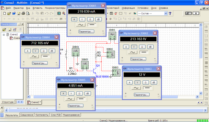
It is worth noting that the gain of one model, depending on a specific instance, can vary by tens or hundreds of times. This necessitates the tuning and adjustment of analog circuits. In this program, fixed coefficients are used in transistor models, I know the logic of their choice. On the MJE18006 in the datasheet, the maximum H21E ratio is 36.
AC amplifier simulation
The given model displays the behavior of the key if an alternating signal and a simple circuit for its inclusion in the circuit are applied to it. It resembles a musical power amplifier circuit.
Usually they use several such series-connected cascades. The number and schemes of cascades, their power circuits depend on the class in which the amplifier operates (A, B, etc.). I will simulate the simplest class A amplifier, which operates in linear mode, as well as take waveforms of input and output voltage.
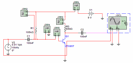
Resistor R1 sets the operating point of the transistor. In the textbooks they write that you need to find such a point on a straight segment of the CVC of the transistor. If the bias voltage is too low, the lower half-wave of the signal will be distorted.
Rpit = (Upit-Ub) / Ib
Ub≈0.7V
Ib = IK / H21E
Capacitors are needed to separate the variable component from the constant. Resistors R2 is installed in order to set the operating mode of the key and set the operating currents. Let's look at the waveforms. We give a signal with an amplitude of 10mV and a frequency of 10,000 Hz. The output amplitude is almost 2V.
Magenta indicates the output waveform, red indicates the input waveform.
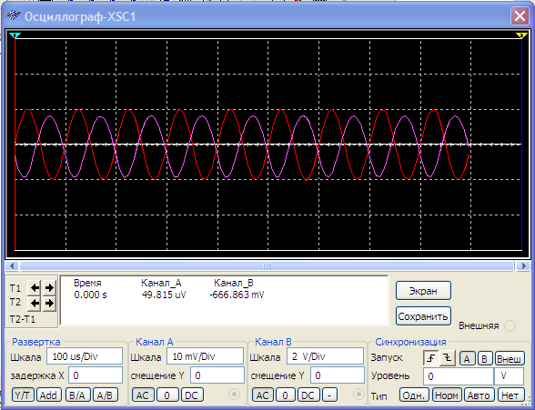
Please note that the signal is inverted, i.e. the output signal is inverted relative to the input. This is a feature of a common emitter circuit. According to the scheme, the signal is removed from the collector. Therefore, when the transistor is opened (when the signal at the input rises), the voltage across it will drop. When the input signal drops, the transistor starts to close and the voltage starts to rise.
This scheme is considered to be the highest quality in terms of signal transmission quality, but you have to pay for this with the power of losses. The fact is that in a state where no signal is input, the transistor is always open and conducts current. Then heat is released:
Ppot = (UKE) / Ik
UKE is a drop on a transistor in the absence of an input signal.
This is the simplest amplifier circuit, while any other circuit works in this way, only the connection of the elements and their combination is different. For example, a Class B transistor amplifier consists of two transistors, each of which works for its own half-wave.
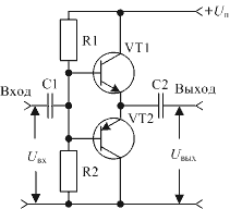
Transistors of different conductivities are used here:
-
VT1 is NPN;
-
VT2 - PNP.
The positive part of the variable input signal opens the upper transistor, and the negative - the lower one.
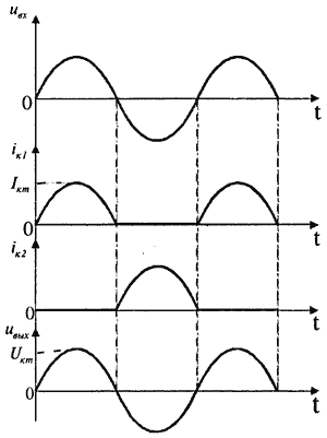
This scheme gives greater efficiency due to the fact that the transistors open and close completely. Due to the fact that when the signal is absent - both transistors are closed, the circuit does not consume current, so there are no losses.
Conclusion
Understanding the operation of the transistor is very important if you are going to do electronics. In this area, it is important not only to learn how to assemble schemes, but also to analyze them. For a systematic study and understanding of devices, you need to understand where and how currents will flow. This will help both in the assembly and in the adjustment and repair of circuits.
It is worth noting that I intentionally omitted many of the nuances and factors so as not to overload the article. At the same time, after the calculations, it’s still pick up resistors. In modeling, this is easy to do. But in practice measure currents and voltages with a multimeter, and ideally need oscilloscopeto check if the input and output waveforms match, otherwise you will have distortion.
See also at bgv.electricianexp.com
:
