Categories: Featured Articles » Novice electricians
Number of views: 157647
Comments on the article: 5
How semiconductor diodes are arranged and work
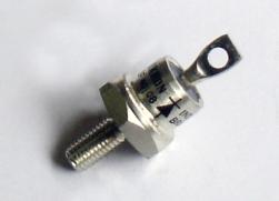 Diodine - the simplest device in the glorious family of semiconductor devices. If we take a plate of a semiconductor, for example Germany, and introduce an acceptor impurity into its left half, and into the right donor one, then on the one hand we get a semiconductor of type P, respectively, on the other type N. In the middle of the crystal we get the so-called P-N junctionas shown in figure 1.
The same figure shows the conditional graphic designation of the diode in the diagrams: the cathode output (negative electrode) is very similar to the “-" sign. It’s easier to remember.
In total, in such a crystal there are two zones with different conductivities, from which two leads come out, so the resulting device is called diodebecause the prefix "di" means two.
In this case, the diode turned out to be a semiconductor, but similar devices were known before: for example, in the era of electronic tubes there was a tube diode called a kenotron. Now such diodes have gone down in history, although adherents of the "tube" sound believe that in a tube amplifier, even the anode voltage rectifier should be a tube!

Figure 1. The structure of the diode and the designation of the diode in the diagram
At the junction of semiconductors with P and N conductivities, it turns out P-N junction (P-N junction), which is the basis of all semiconductor devices. But unlike a diode, in which this transition is only one, transistors have two P-N junctions, and, for example, thyristors consist immediately of four transitions.
P-N transition at rest
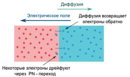
Even if the P-N junction, in this case the diode, is not connected anywhere, all the same, interesting physical processes occur inside it, which are shown in Figure 2.
Figure 2. Diode at rest
In region N there is an excess of electrons, it carries a negative charge, and in region P the charge is positive. Together, these charges form an electric field. Since oppositely charged charges tend to attract, electrons from zone N penetrate into the positively charged zone P, filling some holes with themselves. As a result of such a movement, a current inside the semiconductor, although very small (units of nanoamperes), arises.
As a result of this movement, the density of the substance on the P side increases, but to a certain limit. Particles usually tend to spread uniformly throughout the volume of the substance, similar to how the smell of perfumes spreads throughout the room (diffusion), so, sooner or later, the electrons return back to zone N.
If for most consumers of electricity the direction of the current does not play a role - the light is on, the tile heats up, then for the diode the direction of the current plays a huge role. The main function of the diode is to conduct current in one direction. It is this property that is provided by the P-N junction.
Next, we consider how the diode behaves in two possible cases of connecting a current source.
Turning on the diode in the opposite direction
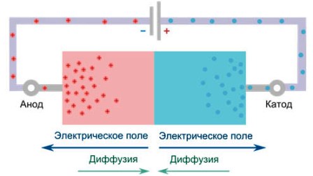
If you connect a power source to the semiconductor diode, as shown in Figure 3, then the current will not pass through the P-N junction.
Figure 3. Reverse diode on
As can be seen in the figure, the positive pole of the power source is connected to region N, and the negative pole to region P. As a result, electrons from region N rush to the positive pole of the source. In turn, positive charges (holes) in region P are attracted by the negative pole of the power source. Therefore, in the region of the P-N junction, as can be seen in the figure, a void forms, there is simply nothing to conduct current, there are no charge carriers.
As the voltage of the power source increases, the electrons and holes are more and more attracted to the electric field of the battery, while in the region of the P – N junction of charge carriers, there is less and less.Therefore, in the reverse connection, the current through the diode does not go. In such cases, it is customary to say that semiconductor diode is closed by reverse voltage.
An increase in the density of matter near the poles of the battery leads to diffusion, - the desire for a uniform distribution of the substance throughout the volume. What happens when you turn off the battery.
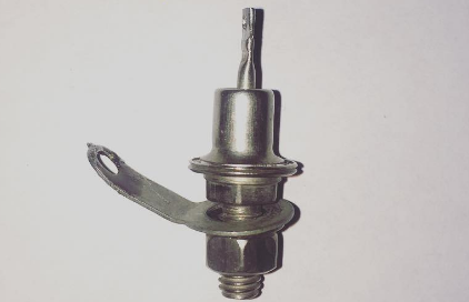
Semiconductor diode reverse current
This is where the time has come to recall the minority carriers, which were conditionally forgotten. The fact is that even in the closed state, an insignificant current passes through the diode, called the reverse current. This reverse current and is created by minority carriers that can move in the same way as the main ones, only in the opposite direction. Naturally, such a motion occurs under reverse voltage. The reverse current, as a rule, is small, due to the small number of minority carriers.
With increasing crystal temperature, the number of minority carriers increases, which leads to an increase in the reverse current, which can lead to the destruction of the P – N junction. Therefore, the operating temperatures for semiconductor devices - diodes, transistors, circuits are limited. In order to prevent overheating, powerful diodes and transistors are installed on heat sinks - radiators.
Turning on the diode in the forward direction
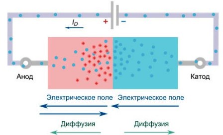
Shown in Figure 4.
Figure 4. Direct turn on diode
Now we change the polarity of the inclusion of the source: minus connect to the region N (cathode), and plus to the region P (anode). With this inclusion in the N region, the electrons will repulse from the minus of the battery, and move towards the P-N junction. In region P, positively charged holes are repelled from the positive terminal of the battery. Electrons and holes rush towards each other.
Charged particles with different polarity are collected near the P-N junction, an electric field arises between them. Therefore, the electrons overcome the P-N junction and continue to move through zone P. At the same time, some of them recombine with holes, but most of them rush to the plus of the battery, current Id goes through the diode.
This current is called direct current. It is limited by the technical data of the diode, some maximum value. If this value is exceeded, there is a danger of the diode breaking down. However, it should be noted that the direction of the forward current in the figure coincides with the generally accepted, reverse motion of electrons.
We can also say that in the forward direction of switching on, the electrical resistance of the diode is relatively small. When you turn it back on, this resistance will be many times greater, the current through the semiconductor diode does not go (a slight reverse current is not taken into account here). From the foregoing, we can conclude that the diode behaves like an ordinary mechanical valve: turned in one direction - water flows, turned in the other - the flow stopped. For this property, the diode is called semiconductor valve.
To understand in detail all the abilities and properties of a semiconductor diode, you should get acquainted with its volt - ampere characteristic. It is also good to learn about the various designs of diodes and frequency properties, about the advantages and disadvantages. This will be discussed in the next article.
Continuation of the article: Characteristics of diodes, designs and application features
Boris Aladyshkin
See also at bgv.electricianexp.com
:

