Categories: Featured Articles » Practical Electronics
Number of views: 411895
Comments on the article: 5
Bipolar Transistor Switching Circuits
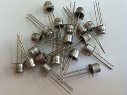 A transistor is a semiconductor device that can amplify, convert and generate electrical signals. The first operational bipolar transistor was invented in 1947. The material for its manufacture was germanium. And already in 1956, a silicon transistor was born.
A bipolar transistor uses two types of charge carriers - electrons and holes, which is why such transistors are called bipolar. In addition to bipolar, there are unipolar (field) transistors in which only one type of carrier is used - electrons or holes. This article will cover bipolar transistors.
Long time transistors they were mainly germanium, and had a p-n-p structure, which was explained by the capabilities of the technologies of that time. But the parameters of germanium transistors were unstable, their biggest drawback is the low operating temperature - not more than 60..70 degrees Celsius. At higher temperatures, transistors became uncontrollable, and then completely failed.
Over time, silicon transistors began to displace germanium counterparts. Currently, they are mainly silicon, and are used, and this is not surprising. After all, silicon transistors and diodes (almost all types) remain operational up to 150 ... 170 degrees. Silicon transistors are also the "stuffing" of all integrated circuits.
Transistors are rightfully considered one of the great discoveries of mankind. Having replaced the electronic lamps, they not only replaced them, but made a revolution in electronics, surprised and shocked the world. If there were no transistors, then many modern devices and devices, so familiar and close, simply would not have been born: imagine, for example, a mobile phone with electronic lamps! See transistor history for more information. here.
Most silicon transistors have an n-p-n structure, which is also explained by the production technology, although there are silicon p-n-p type transistors, but they are slightly smaller than the n-p-n structures. Such transistors are used as part of complementary pairs (transistors of different conductivity with the same electrical parameters). For example, KT315 and KT361, KT815 and KT814, and in the output stages of transistor UMZCH KT819 and KT818. In imported amplifiers, a powerful complementary pair of 2SA1943 and 2SC5200 is very often used.
Often, transistors of a p-n-p structure are called forward conductivity transistors, and n-p-n structures are reverse transistors. For some reason, such a name is almost never found in the literature, but in the circle of radio engineers and radio enthusiasts it is used everywhere, everyone immediately understands what is at stake. Figure 1 shows a schematic structure of transistors and their graphic symbols.
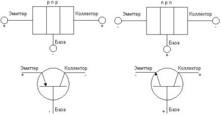
Picture 1.
In addition to differences in conductivity type and material, bipolar transistors are classified by power and operating frequency. If the dissipation power on the transistor does not exceed 0.3 W, such a transistor is considered low-power. With a power of 0.3 ... 3 W, the transistor is called a medium power transistor, and with a power of more than 3 W, the power is considered large. Modern transistors are able to dissipate power of several tens or even hundreds of watts.
Transistors amplify electrical signals not equally well: with increasing frequency, the gain of the transistor stage drops, and at a certain frequency it stops altogether. Therefore, to operate in a wide range of frequencies, transistors are available with different frequency properties.
According to the operating frequency, transistors are divided into low-frequency ones, - the operating frequency is not more than 3 MHz, the mid-frequency - 3 ... 30 MHz, high-frequency - over 30 MHz.If the operating frequency exceeds 300 MHz, then these are microwave transistors.
In general, in serious thick reference books there are more than 100 different parameters of transistors, which also indicates a huge number of models. And the number of modern transistors is such that in full they can no longer be placed in any directory. And the lineup is constantly growing, allowing us to solve almost all the tasks set by the developers.
There are many transistor circuits (just remember the number of at least household equipment) for amplifying and converting electrical signals, but, with all the diversity, these circuits consist of separate stages, the basis of which are transistors. To achieve the necessary signal amplification, it is necessary to use several stages of amplification, connected in series. To understand how amplifier stages work, you need to become more familiar with transistor switching circuits.
The transistor alone cannot amplify anything. Its amplifying properties are that small changes in the input signal (current or voltage) lead to significant changes in voltage or current at the output of the cascade due to the expenditure of energy from an external source. It is this property that is widely used in analog circuits - amplifiers, television, radio, communication, etc.
To simplify the presentation, we will consider circuits on transistors of the n-p-n structure here. Everything that will be said about these transistors applies equally to p-n-p transistors. Just change the polarity of the power sources, electrolytic capacitors and diodesif any, to get a working circuit.
Transistor Switching Circuits
There are three such schemes in total: a circuit with a common emitter (OE), a circuit with a common collector (OK), and a circuit with a common base (OB). All these schemes are shown in Figure 2.
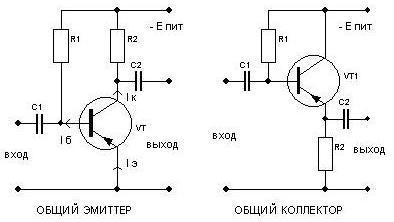
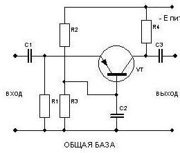
Figure 2
But before moving on to considering these circuits, you should get acquainted with how the transistor works in key mode. This acquaintance should facilitate understanding. transistor operation in gain mode. In a certain sense, a key scheme can be considered as a kind of scheme with MA.
Transistor operation in key mode
Before studying the operation of a transistor in signal amplification mode, it is worth remembering that transistors are often used in key mode.
This mode of operation of the transistor has been considered for a long time. In the August 1959 issue of Radio magazine, an article by G. Lavrov “Semiconductor triode in key mode” was published. The author of the article suggested adjust the speed of the collector motor change in the duration of the pulses in the control winding (OS). Now, this method of regulation is called PWM and is used quite often. The diagram from the journal of that time is shown in Figure 3.
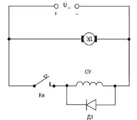
Figure 3
But key mode is used not only in PWM systems. Often a transistor just turns something on and off.
In this case, the relay can be used as a load: they gave an input signal - the relay turned on, no - the relay signal turned off. Instead of relays in key mode, light bulbs are often used. Usually this is done to indicate: the light is either on or off. A diagram of such a key stage is shown in Figure 4. Key stages are also used for working with LEDs or optocouplers.
Figure 4
In the figure, the cascade is controlled by a normal contact, although there may be a digital chip or microcontroller. Automobile light bulb, this one is used to illuminate the dashboard in the "Lada". It should be noted that 5V is used for control, and the commutated collector voltage is 12V.
There is nothing strange in this, since voltages do not play any role in this circuit, only currents are of importance.Therefore, the bulb can be at least 220V if the transistor is designed to operate at such voltages. The voltage of the collector source must also correspond to the operating voltage of the load. With the help of such cascades, the load is connected to digital microcircuits or microcontrollers.
In this scheme, the base current controls the collector current, which, due to the energy of the power supply, is several tens or even hundreds of times (depending on the collector load) than the base current. It is easy to see that current amplification occurs. When the transistor is in the key mode, they usually use a value called a current gain in the large signal mode in the reference books to calculate the cascade — it is indicated by the letter β in the reference books. This is the ratio of the collector current, determined by the load, to the minimum possible base current. In the form of a mathematical formula, it looks like this: β = Iк / Iб.
For most modern transistors, the coefficient β it is quite large, as a rule, from 50 and higher, therefore, when calculating the key stage, it can be taken as only 10. Even if the base current turns out to be larger than the calculated one, the transistor will not open more from this, then it is also a key mode.
To light the bulb shown in Figure 3, Ib = Ik / β = 100mA / 10 = 10mA, this is at least. With a control voltage of 5 V at the base resistor RB, minus the voltage drop in the BE section, 5 V - 0.6 V = 4.4 V will remain. The resistance of the base resistor is: 4.4V / 10mA = 440 Ohm. A resistor with a resistance of 430 ohms is selected from the standard series. A voltage of 0.6 V is the voltage at the B – E junction, and should not be forgotten in the calculations!
In order to prevent the transistor base from “hanging in the air” when opening the control contact, the B – E transition is usually shunted by the resistor Rbe, which reliably closes the transistor. This resistor should not be forgotten, although for some reason it is not for some reason, which can lead to a false operation of the cascade from interference. Actually, everyone knew about this resistor, but for some reason they forgot, and once again stepped on the "rake".
The value of this resistor must be such that when the contact opens, the voltage at the base does not turn out to be less than 0.6V, otherwise the cascade will be uncontrollable, as if section B – E were simply short-circuited. In practice, the RBe resistor is set at a value of about ten times more than RB. But even if the Rb value is 10K, the circuit will work reliably enough: the base and emitter potentials will be equal, which will lead to the closing of the transistor.
Such a key cascade, if it is working, can turn on the light bulb in full heat, or turn it off completely. In this case, the transistor can be fully open (saturation state) or completely closed (cut-off state). Immediately, of course, the conclusion suggests itself that between these "boundary" states there is such a thing when the bulb shines completely. In this case, is the transistor half open or half closed? It’s like in the problem of filling the glass: the optimist sees the glass half full, while the pessimist considers it half empty. This mode of operation of the transistor is called amplifying or linear.
Transistor operation in signal amplification mode
Almost all modern electronic equipment consists of microcircuits in which transistors are “hidden”. Simply select the operating mode of the operational amplifier to obtain the desired gain or bandwidth. But, despite this, cascades are often used on discrete (“loose”) transistors, and therefore, an understanding of the operation of the amplifier stage is simply necessary.
The most common inclusion of a transistor compared to OK and OB is a common emitter (OE) circuit. The reason for this prevalence is, first of all, a high gain in voltage and current.The highest gain of the OE cascade is achieved when half the voltage of the power supply Epit / 2 drops at the collector load. Accordingly, the second half falls on the KE section of the transistor. This is achieved by setting up the cascade, which will be described below. This gain mode is called Class A.
When you turn on the transistor with the OE, the output signal on the collector is in antiphase with the input. As disadvantages, it can be noted that the input impedance of the OE is small (not more than a few hundred Ohms), and the output impedance is in the range of tens of KOhms.
If in the key mode the transistor is characterized by a current gain in large signal mode β, then in the gain mode, the "current gain in the small signal mode" is used, denoted in the h21e reference books. This designation came from the representation of a transistor in the form of a four-terminal device. The letter “e” indicates that the measurements were made when the transistor with a common emitter was turned on.
The coefficient h21e, as a rule, is somewhat larger than β, although in calculations, as a first approximation, you can use it. Anyway, the scatter of the parameters β and h21e is so large even for one type of transistor that the calculations are only approximate. After such calculations, as a rule, the configuration of the circuit is required.
The gain of the transistor depends on the thickness of the base, so you cannot change it. Hence the large spread of the gain of transistors taken even from one box (read one batch). For low-power transistors, this coefficient varies between 100 ... 1000, and for powerful 5 ... 200. The thinner the base, the higher the ratio.
The simplest turn-on circuit for an OE transistor is shown in Figure 5. This is just a small piece from Figure 2, shown in the second part of the article. This circuit is called a fixed base current circuit.

Figure 5
The scheme is extremely simple. The input signal is supplied to the base of the transistor through an isolation capacitor C1, and, being amplified, is removed from the collector of the transistor through a capacitor C2. The purpose of the capacitors is to protect the input circuits from the constant component of the input signal (just remember the carbon or electret microphone) and provide the necessary bandwidth of the cascade.
Resistor R2 is the collector load of the cascade, and R1 supplies a constant bias to the base. Using this resistor, they try to make the collector voltage Epit / 2. This condition is called the operating point of the transistor, in this case the gain of the cascade is maximum.
Approximately the resistance of the resistor R1 can be determined by the simple formula R1 ≈ R2 * h21e / 1.5 ... 1.8. The coefficient 1.5 ... 1.8 is substituted depending on the supply voltage: at low voltage (not more than 9V), the coefficient value is not more than 1.5, and starting from 50V, it approaches 1.8 ... 2.0. But, indeed, the formula is so approximate that the resistor R1 most often has to be selected, otherwise the required value of Epit / 2 on the collector will not be obtained.
The collector resistor R2 is set as a condition of the problem, since the collector current and the amplification of the cascade as a whole depend on its magnitude: the greater the resistance of the resistor R2, the higher the gain. But you need to be careful with this resistor, the collector current must be less than the maximum permissible for this type of transistor.
The scheme is very simple, but this simplicity gives it negative properties, and you have to pay for this simplicity. Firstly, the amplification of the cascade depends on the specific instance of the transistor: it replaced the transistor during repair, - select the offset again, output it to the operating point.
Secondly, from the ambient temperature, - with increasing temperature, the collector reverse current Ico increases, which leads to an increase in the collector current. And where, then, is half the supply voltage on the Epit / 2 collector, the same operating point? As a result, the transistor heats up even more, after which it fails.To get rid of this dependence, or at least minimize it, additional elements of negative feedback — OOS — are introduced into the transistor cascade.
Figure 6 shows a circuit with a fixed bias voltage.

Figure 6
It would seem that the voltage divider Rb-k, Rb-e will provide the required initial displacement of the cascade, but in fact such a cascade has all the disadvantages of a fixed current circuit. Thus, the circuit shown is just a variation of the fixed current circuit shown in Figure 5.
Schemes with thermal stabilization
The situation is somewhat better in the case of applying the schemes shown in Figure 7.

Figure 7
In a collector-stabilized circuit, the bias resistor R1 is connected not to the power source, but to the collector of the transistor. In this case, if the temperature increases, the reverse current increases, the transistor opens stronger, the collector voltage decreases. This decrease leads to a decrease in the bias voltage supplied to the base through R1. The transistor starts to close, the collector current decreases to an acceptable value, the position of the operating point is restored.
It is obvious that such a stabilization measure leads to a certain decrease in the amplification of the cascade, but this does not matter. The missing gain is usually added by increasing the number of amplification stages. But such an environmental protection system can significantly expand the range of operating temperatures of the cascade.
The circuitry of the cascade with emitter stabilization is somewhat more complicated. The amplifying properties of such cascades remain unchanged in an even wider temperature range than in the collector-stabilized circuit. And one more indisputable advantage - when replacing a transistor, you do not have to re-select the cascade operating modes.
The emitter resistor R4, providing temperature stabilization, also reduces the gain of the cascade. This is for direct current. In order to exclude the influence of resistor R4 on the amplification of alternating current, resistor R4 is bridged by capacitor Ce, which is an insignificant resistance for alternating current. Its value is determined by the frequency range of the amplifier. If these frequencies lie in the sound range, then the capacitance of the capacitor can be from units to tens or even hundreds of microfarads. For radio frequencies, this is already hundredths or thousandths, but in some cases the circuit works fine even without this capacitor.
In order to better understand how emitter stabilization works, you need to consider the circuit for switching on a transistor with a common OK collector.
The common collector (OK) circuit is shown in Figure 8. This circuit is a slice of Figure 2, from the second part of the article, where all three transistor switching circuits are shown.

Figure 8
The cascade is loaded by the emitter resistor R2, the input signal is supplied through the capacitor C1, and the output signal is removed through the capacitor C2. Here you can ask, why is this scheme called OK? Indeed, if we recall the OE circuit, it is clearly visible there that the emitter is connected to a common circuit wire, relative to which the input signal is supplied and the output signal is taken.
In the OK circuit, the collector is simply connected to a power source, and at first glance it seems that it has nothing to do with the input and output signal. But in fact, the EMF source (power battery) has a very small internal resistance, for a signal it is almost one point, one and the same contact.
In more detail, the operation of the OK circuit can be seen in Figure 9.

Figure 9
It is known that for silicon transistors the voltage of the bi-e transition is in the range of 0.5 ... 0.7 V, so you can take it on average 0.6 V, if you do not set the goal to carry out calculations with an accuracy of tenths of a percent. Therefore, as can be seen in Figure 9, the output voltage will always be less than the input voltage by the value of Ub-e, namely, those same 0.6V.Unlike the OE circuit, this circuit does not invert the input signal, it simply repeats it, and even reduces it by 0.6V. This circuit is also called an emitter follower. Why is such a scheme needed, what is its use?
The OK circuit amplifies the current signal h21e times, which indicates that the input resistance of the circuit is h21e times larger than the resistance in the emitter circuit. In other words, without fear of burning the transistor, you can apply voltage directly to the base (without a limiting resistor). Just take the base pin and connect it to the + U power bus.
A high input impedance allows you to connect a high impedance input source (complex impedance), such as a piezoelectric pickup. If such a pickup is connected to the cascade according to the OE scheme, then the low input impedance of this cascade simply “lands” the pickup signal - “the radio will not play”.
A distinctive feature of the OK circuit is that its collector current Ik depends only on the load resistance and voltage of the input signal source. At the same time, the parameters of the transistor do not play any role at all. They say about such circuits that they are covered by one hundred percent voltage feedback.
As shown in Figure 9, the current in the emitter load (it is the emitter current) In = Ik + Ib. Taking into account that the base current Ib is negligible compared to the collector current Ik, we can assume that the load current is equal to the collector current Iн = Iк. The current in the load will be (Uin - Ube) / Rн. In this case, we assume that Ube is known and is always equal to 0.6V.
It follows that the collector current Ik = (Uin - Ube) / Rn depends only on the input voltage and load resistance. The load resistance can be changed within wide limits, however, it is not necessary to particularly zealous. Indeed, if instead of Rн we put a nail - a hundredth, then no transistor can stand it!
The OK circuit makes it quite easy to measure the static current transfer coefficient h21e. How to do this is shown in Figure 10.

Figure 10
First, measure the load current as shown in Figure 10a. In this case, the base of the transistor does not need to be connected anywhere, as shown in the figure. After that, the base current is measured in accordance with Figure 10b. Measurements should in both cases be carried out in the same quantities: either in amperes or in milliamperes. The power supply voltage and load should remain unchanged in both measurements. To find out the static coefficient of current transfer, it is enough to divide the load current by the base current: h21e ≈ In / IB.
It should be noted that with an increase in the load current, h21e decreases slightly, and with an increase in the supply voltage it increases. Emitter repeaters are often built on a push-pull circuit using complementary pairs of transistors, which allows to increase the output power of the device. Such an emitter follower is shown in Figure 11.

Figure 11.
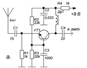
Figure 12.
Turning on transistors according to a scheme with a common OB base
Such a circuit provides only voltage gain, but has better frequency properties compared to the OE circuit: the same transistors can operate at higher frequencies. The main application of the OB scheme is the UHF antenna amplifiers. A diagram of the antenna amplifier is shown in Figure 12.
See also at bgv.electricianexp.com
:

