Categories: Featured Articles » Practical Electronics
Number of views: 162,409
Comments on the article: 5
Comparator circuits
How does the voltage comparator
 In many descriptions, the comparator is compared with conventional lever scales, as in a bazaar: a standard is placed on one bowl - weights, and the seller begins to put goods, such as potatoes, on the other. As soon as the weight of the product becomes equal to the weight of the weights, more precisely a little more, the cup with weights rushes up. Weighing is over.
The same thing happens with the comparator, only in this case the role of weights is played by the reference voltage, and the input signal is used as a potato. As soon as a logical unit appears at the output of the comparator, it is considered that the voltage comparison has occurred. This is the very “a bit more”, which in the directories is called the “threshold sensitivity of the comparator”.
Voltage Comparator Check
Novice hams - electronics engineers often ask how to check a particular part. To check the comparator, you do not need to assemble any complex circuit. It is enough to connect a voltmeter to the output of the comparator, and apply regulated voltages to the inputs, and determine whether the comparator is working or not. And, of course, it will be very good, if you still remember to apply power to the comparator!
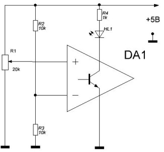
However, one should not forget that many comparators have an output transistor, in which the findings of the collector and emitter simply "hang in the air", which was described in the article "Analog Comparators". Therefore, these conclusions must be connected accordingly. How to do this is shown in Figure 1.
Figure 1. Comparator connection diagram
The reference voltage obtained from divider R2, R3 from supply voltage + 5V. As a result, 2.5V is obtained at the inverse input. Suppose that the variable resistor R1 slider is in the lowest position, i.e. voltage on it is 0V. The same voltage is at the direct input of the comparator.
If now, by rotating the variable resistor R1 engine, gradually increase the voltage at the direct input of the comparator, then when 2.5V is reached, logic 1 will appear at the output of the comparator, which will open the output transistor, the HL1 LED will light.
If now the engine R1 is rotated in the direction of decreasing voltage, then at a certain moment the LED HL1 will undoubtedly go out. This indicates the proper operation of the comparator.
The experiment can be somewhat complicated: measure the voltage at the direct input of the comparator with a voltmeter, and fix at what voltage the LED will light up and at which it goes out. The difference in these voltages will be the hysteresis of the comparator. By the way, some comparators have a special pin (pin) for adjusting the hysteresis value.
To conduct such an experiment, you will need a digital voltmeter capable of "catching" millivolts, a multi-turn trimming resistor and a fair amount of patience for the performer. If patience for such an experiment is not enough, you can do the following, which is much simpler: swap the direct and inverse inputs, and rotate the variable resistor to observe how the LED behaves, i.e. comparator output.
Figure 1 shows just a block diagram, so the pin numbers are not indicated. When checking a real comparator, you will have to deal with its pinout (pinout). Next, some practical schemes will be considered and a brief description of their work will be given.
Often in one case there are several comparators, two or four, which allows you to create different devices without installing extra chips on the board. Comparators can be independent of each other, but in some cases have internal connections. As such a chip, consider the MAX933 dual comparator.
Comparator MAX933
Two comparators “live” in one housing of the microcircuit. In addition to the comparators themselves, there is a built-in 1.182V voltage reference source inside the microcircuit. In the figure, it is shown in the form of a zener diode, which is already connected inside the microcircuit: to the upper comparator to the inverse input, and to the bottom to the straight line. This makes it easy to create a multi-level comparator according to the principles of "Little", "Norm", "Many" (undervoltage / overvoltage detectors). Such comparators are called windowed because the “norm” position is in the “window” between “few” and “many”.
Study comparator program Multisim
Figure 2 shows the measurement of the reference voltage produced using the Multisim simulation software. The measurement is carried out with an XMM2 multimeter, which shows 1.182V, which fully corresponds to the value specified in the Data Sheet of the comparator. Pin 5 HYST, - hysteresis adjustment, in this case is not used.
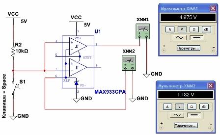
Figure 2
Using switch S1, you can set the input voltage level, and, at once, on both comparators: a closed switch supplies a low level to the inputs (less than the reference voltage) as shown in Figure 3, an open state corresponds to a high level, - Figure 4. State of the outputs of the comparators shown by multimeters XMM1, XMM2.
Comments on the figures are completely redundant - to understand the logic of the comparators, it is enough to carefully consider the readings of the multimeters and the position of the switch S1. It should only be added that such a scheme can be recommended for checking a real "iron" comparator.
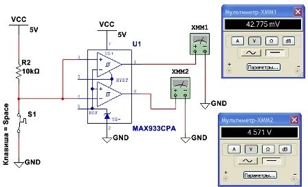
Figure 3
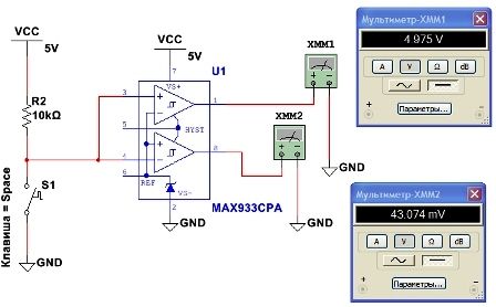
Figure 4
Voltage test circuit
The circuit of such a comparator shown in the Data Sheet is shown in Figure 5.
For output signals of undervoltage (OUTA) and overvoltage (OUTB), the active signal level is low, which is indicated by underlining the signals from above. Sometimes for these purposes the sign “-” or “/” in front of the signal name is used. These signals can be called alarms.
POWER GOOD signal is output logical element ANDwhen both alarms have a logical unit level. The active POWER GOOD signal is high.
If at least one of the alarms is low, the POWER GOOD signal will disappear - it will also become low. This once again makes it possible to verify that the logical circuit AND for low levels is a logical OR.
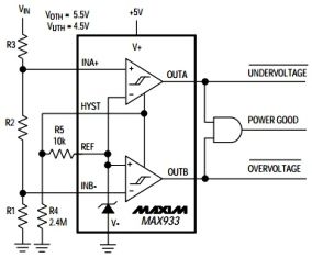
Figure 5. Comparator circuit
The controlled input voltage is supplied through the divider R1 ... R3, the value of the resistors of which is calculated taking into account the range of controlled voltages. The calculation procedure is given, even with an example, in the Data Sheet.
To reduce chatter during switching, the hysteresis value is set using the divider R4, R5. These resistors are calculated using the formulas also given in the Data Sheet. For the values indicated in the diagram, the hysteresis value is 50mV.
Backup Management Scheme
Similar schemes are used, for example, in alarm systems. The operation algorithm of these schemes is quite simple. If the mains voltage fails, the security system switches to battery operation, and when the network is restored, it again works from the power supply, while the battery is being charged. To implement such an algorithm, at least two factors must be evaluated: the presence of mains voltage and the state of the battery.
The functional control circuit is shown in Figure 6.
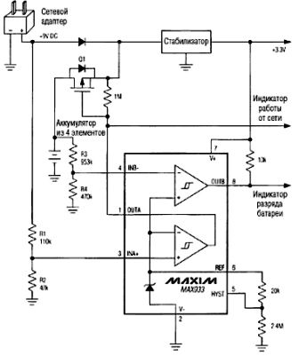
Figure 6. The backup power management scheme on a single chip
The rectified voltage + 9VDC is supplied through the diode to the voltage regulator, from which the security device is powered. In this case, the divider R1, R2 is a line voltage sensor, which is monitored by the lower comparator with OUTA output. When there is mains voltage, and is within reason, at the output of the lower comparator, a logic unit that opens the field-effect transistor Q1, through which the battery is charged. The same signal controls the network operation indicator.
In the event that the mains voltage disappears or decreases, a logical zero appears at the output of the comparator, the field-effect transistor closes, the battery stops charging, the network operation indicator goes off or turns a different color. The appearance of a sound signal is also possible.
A charged battery through a switching diode is connected to the stabilizer, and the device continues to work offline. But in order to protect the battery from a full discharge, another comparator monitors its condition, the top one according to the scheme.
While the battery has not yet discharged, the voltage at the inverse input of comparator B is higher than the reference, therefore, the output level of the comparator is low, which corresponds to the normal charge of the batteries. As the discharge occurs, the voltage at the divider R3, R4 drops, and when it becomes lower than the reference, a high level will be established at the output of the comparator, which indicates a low battery. Most often, this condition is indicated by the annoying squeak of the device.
Time delay circuit
Shown in Figure 7.
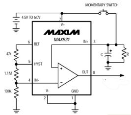
Figure 7. Scheme of time delay on the comparator
The scheme works as follows. By pressing the MOMENTARY SWITCH button, capacitor C is charged to the voltage of the power source. This leads to the fact that the voltage at the input IN + becomes higher than the reference voltage at the input IN-. Therefore, the output OUT is set to a high level.
After releasing the button, the capacitor begins to discharge through the resistor R, and when the voltage on it, and, therefore, at the input IN + drops below the reference voltage at the input IN-, the output level of the comparator OUT will be low. When you press the button again, everything repeats again.
The reference voltage at the input IN- is set using a divider of three resistors and with the values indicated on the diagram is 100mV. The same divider sets the hysteresis of the comparator (HYST) within 50mV. Thus, the capacitor C is discharged to a voltage of 100 - 50 = 50 mV.
The current consumption of the device itself is small, no more than 35 microamps, while the output current can reach 40 mA.
The time delay is calculated by the formula R * C * 4.6 sec. An example is the calculation with the following data: 2M & # 937; * 10µF * 4.6 = 92 sec. If the resistance is indicated in megaohms, the capacitance is in microfarads, then the result is obtained in seconds. But this is only a calculated result. Actual time will depend on the voltage of the power source and on the quality of the capacitor, on its leakage current.
Some simple comparator circuits
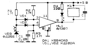
The basis of the circuits, which will be considered later, is a gradient relay, a circuit that reacts not to the presence of any signal, but to the rate of its change. One of these sensors is photo relaywhose diagram is shown in Figure 8.
Figure 8. Scheme of the photo relay on the comparator
The input signal is obtained from the divider formed by the resistor R1 and the photodiode VD3. The common point of this divider through the diodes VD1 and VD2 is connected to the direct and inverting input of the comparator DA1. Thus, it turns out that the direct and inverse inputs have the same voltage, i.e. there is no difference between the voltages at the inputs. With this state at the inputs, the sensitivity of the comparator is close to maximum.
To change the state of the comparator, the voltage difference at the inputs in units of millivolts will be required. This is about how to push your little finger into the abyss hanging on the edge of a stone. In the meantime, a logical zero is present at the output of the comparator.
If the illumination suddenly changes, the voltage on the photodiode also changes, suppose that it increases. It would seem that along with this the voltage at both inputs of the comparator will change, and immediately. Therefore, the desired voltage difference at the inputs will not work, and, therefore, the state of the output of the comparator will not change.
All this would be so, if you do not pay attention to the capacitor C1 and the resistor R3. Thanks to this RC circuit, the voltage at the inverted input of the comparator will increase with some delay relative to the direct input. For the delay time, the voltage at the direct input will be greater than at the inverse. As a result, a logical unit will appear at the output of the comparator. This unit will not be held for long, just for the delay time due to the RC chain.
A similar photo relay is used in cases where the illumination changes quickly enough. For example, in security devices or sensors of finished products on conveyors, the device will respond to interruption of the light flux. Another option is as an addition to the video surveillance system. If you direct the photosensor to the monitor screen, it will detect a change in brightness and turn on, for example, an audio signal, attracting the attention of the operator.
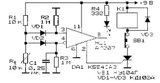
It is very simple to turn the considered photo relay into a temperature change sensor, for example, in fire alarm. To do this, just replace the photodiode with a thermistor. In this case, the value of the resistor R1 must be equal to the value of the thermistor (usually indicated for a temperature of 25C °). A diagram of this sensor is shown in Figure 9.
Figure 9. Diagram of a temperature measuring sensor on a comparator
The principle and meaning of the work is exactly the same as that of the photosensor described above. But this design also shows the simplest output device - this is the thyristor VS1 and relay K1. When the comparator is triggered, the thyristor VS1 opens, which turns on the relay K1.
Since the thyristor in this case operates in a direct current circuit, even when the control pulse from the comparator ends, the thyristor will remain open, and relay K1 turned on. To turn off the relay, you will have to press the SB1 button or simply turn off the entire circuit.
Instead of a thermistor, you can use a magnetoresistor, for example SM-1, reacting to a magnetic field. Then you get a magnetically sensitive gradient relay. Magnetoresistors in the last XX century were used in the keyboards of some computers.
If you use other sensors, then on the basis of the gradient relay, you can easily make completely different devices that respond to changes in the electric field, to sound vibrations. Using piezoelectric sensors, it is easy to create shock sensors and seismic vibrations.
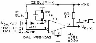
It is quite simple with the help of comparators to convert the “analog” signal into a “digital” one. A similar scheme is shown in Figure 10.
Figure 10. Scheme for converting an “analog” signal to a “digital” signal using a comparator
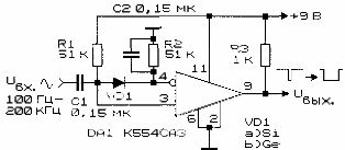
Figure 11 shows the same circuit, only the polarity of the output pulses is inverse to the previous one. This is achieved simply by the inclusion of other inputs.
Figure 11.
Both circuits convert the amplitude of the input signal to the width of the output pulse. Such a conversion is often used in various electronic circuits. First of all, in measuring devices, switching power supplies, digital amplifiers.
The frequency range of the devices is in the range of 5 ... 200KHz, the amplitude of the input signal in the range of 2 ... 2.5V. When using a germanium diode, the conversion of the amplitude to the pulse width starts from the level of 80 ... 90mV, while for a silicon diode this value is 250 ... 270mV.
The operating frequency band of the device is determined by the ratings of capacitors C1, C2. A device assembled from serviceable parts does not require adjustment and setting a response threshold.
See also at bgv.electricianexp.com
:

