Categories: Featured Articles » Practical Electronics
Number of views: 113767
Comments on the article: 5
Integrated timer NE555 - history, design and operation
The history of the creation of a very popular chip and a description of its internal structure
 One of the legends of electronics is integrated circuit chip NE555. It was developed back in 1972. Such longevity is far from every chip and not even every transistor can be proud of. So what is so special about this microcircuit, which has three fives in its marking?
Signetics Launches Series Production of NE555 Chip exactly one year after it was developed by Hans R. Kamensind. The most amazing thing in this story was that at that time Kamensind was practically unemployed: he quit PR Mallory, but did not manage to get anywhere. In fact, it was a “homework”.
The chip saw the light of the day and gained such great fame and popularity thanks to the efforts of Signetics manager Art Fury, who was, of course, a friend of Kamensind. He used to work for General Electric, so he knew the electronics market what was needed there and how to attract the attention of a potential buyer.
According to the memoirs of Kamensinda A. Fury was a true enthusiast and lover of his craft. At home, he had a whole laboratory filled with radio components, where he conducted various studies and experiments. This made it possible to accumulate vast practical experience and deepen theoretical knowledge.
At that time, Signetics products were called “5 **”, and the experienced A. Fury, who had a supernatural sense of the electronics market, decided that marking 555 (three fives) would be most welcome for the new chip. And he was not mistaken: the microcircuit went simply like hot cakes, it became perhaps the most massive in the entire history of the creation of microcircuits. The most interesting thing is that the microcircuit has not lost its relevance to this day.
Somewhat later, two letters appeared in the marking of the microcircuit, it became known as NE555. But since in those days there was a complete mess in the patenting system, the integrated timer rushed to release everyone who is not lazy, naturally, putting three letters (read yours) in front of three fives. Later, based on the 555 timer, dual (IN556N) and quadruple (IN558N) timers were developed, naturally, in more multi-pin cases. But the basis was still the same NE555.
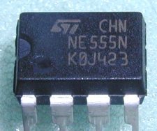
Fig. 1. Integrated timer NE555
555 in the USSR
The first description of 555 in the domestic radio-technical literature appeared already in 1975 in the journal Electronics. The authors of the article noted the fact that this chip will enjoy no less popularity than the widely known operational amplifiers at that time. And they were not at all mistaken. The microcircuit made it possible to create very simple designs, and almost all of them started working immediately, without painful adjustment. But it is known that the repeatability of the design at home increases in proportion to the square of its “simplicity”.
In the Soviet Union in the late 80s, a complete analogue of 555 was developed, called KR1006VI1. The first industrial application of the domestic analogue was in the VCR12 Electronics video recorder.
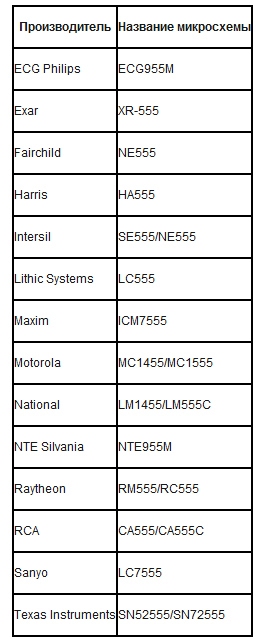
Chip manufacturers NE555:

Internal device chip NE555
Before grabbing the soldering iron and starting the assembly of the structure on the integral timer, let's first figure out what is inside and how it all works. After that, it will be much easier to understand how a specific practical scheme works.
The integrated timer contains over twenty transistorsthe connection of which is shown in the figure - https://env.electricianexp.com/555ic.jpg
As you can see, the circuit diagram is quite complex, and is given here only for general information.After all, you can’t get into it with a soldering iron anyway, you won’t be able to repair it. As a matter of fact, this is exactly what all other microcircuits, both digital and analog, look from the inside (see - Legendary Analog Chips) Such is the technology for the production of integrated circuits. It will also not be possible to understand the logic of the device as a whole by such a scheme, therefore the functional scheme is shown below and its description is given.
Technical details
But, before you deal with the logic of the chip, you should probably bring its electrical parameters. The range of supply voltages is wide enough 4.5 ... 18V, and the output current can reach 200mA, which allows the use of even low-power relays as a load. The chip itself consumes very little: only 3 ... 6 mA is added to the load current. At the same time, the accuracy of the timer itself is practically independent of the supply voltage, - only 1 percent of the calculated value. The drift is only 0.1% / volt. The temperature drift is also small - only 0, 005% / ° C. As you can see, everything is quite stable.
Functional diagram of NE555 (KR1006VI1)
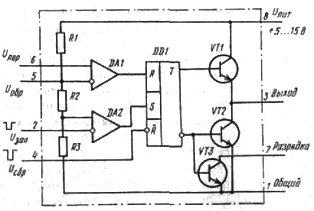
As mentioned above, in the USSR they made an analogue of the bourgeois NE555 and called it KR1006VI1. The analogue turned out to be very successful, no worse than the original, so you can use it without any fear or doubt. Figure 3 shows the functional diagram of the integrated timer KR1006VI1. It is fully consistent with the NE555 chip.
Figure 3. Functional diagram of the integrated timer KR1006VI1
The chip itself is not so big - it is available in an eight-pin DIP8 package, as well as in a small-sized SOIC8. The latter suggests that 555 can be used for SMD editing, in other words, developers still have an interest in it.
There are also few elements inside the microcircuit. The main one is the most common RS is a trigger DD1. When a logical unit is fed to input R, the trigger is reset to zero, and when a logical unit is fed to input S, it is naturally set to one. To generate control signals on the RS - inputs special circuit on comparators, which will be discussed a little later.
The physical levels of a logical unit depend, of course, on the used supply voltage and practically range from Upit / 2 to almost full Upit. Approximately the same ratio is observed for logic microcircuits of the CMOS structure. Logical zero is, as usual, within 0 ... 0.4V. But these levels are inside the microcircuit, you can only guess about them, but you can’t feel them with your hands, you can’t see with your eyes.
Output stage
To increase the load capacity of the chip, a powerful output stage on transistors VT1, VT2 is connected to the output of the trigger.
If the RS - trigger is reset, then the output (pin 3) contains a logic zero voltage, i.e. open transistor VT2. In the case when the trigger is installed at the output, the level of the logical unit is also.
The output stage is made by a push-pull circuit, which allows you to connect the load between the output and the common wire (terminals 3.1) or the power bus (terminals 3.8).
A small remark on the output stage. When repairing and adjusting devices on digital microcircuits, one of the methods for checking the circuit is to supply a low level signal to the inputs and outputs of the microcircuits. As a rule, this is done by shorting to the common wire of these inputs and outputs with the help of a sewing needle, while not causing any harm to the microcircuit.
In some circuits, the NE555 power supply is 5V, so it seems that this is also digital logic and you can do it quite freely too. But actually it is not. In the case of the 555 chip, or rather, with its push-pull output, such “experiments” cannot be done: if the output transistor VT1 is at this moment open, then a short circuit will result and the transistor will simply burn out. And if the supply voltage is close to maximum, then a deplorable ending is simply inevitable.
Additional transistor (pin 7)
In addition to the mentioned transistors, there is also a transistor VT3. The collector of this transistor is connected to the output of the chip 7 "Discharge". Its purpose is to discharge the time-setting capacitor when using the microcircuit as a pulse generator. The discharge of the capacitor occurs when the trigger DD1 is reset. If we recall the description of the trigger, then at the inverse output (indicated by a circle in the diagram) at this moment there is a logical unit, leading to the opening of the transistor VT3.
About the reset signal (pin 4)
You can reset a trigger at any time - the “reset” signal has a high priority. To do this, there is a special input R (pin 4), indicated in the figure as Usbr. As can be understood from the figure, a reset will occur if a low-level pulse of not more than 0.7V is applied to the 4th output. At the same time, a low level voltage will appear at the output of the microcircuit (pin 3).
In cases where this input is not used, the logic unit level is applied to it to get rid of impulse noise. The easiest way to do this is by connecting pin 4 directly to the power bus. In no case should you leave it, as they say, in the "air". Then you will have to wonder and think for a long time, and why does the circuit work so unstably?
General trigger notes
In order not to be completely confused about the state of the trigger, it should be recalled that in discussions about the trigger the state of its direct exit is always taken into account. Well, if it is said that the trigger is “installed”, then on the direct output the state of the logical unit. If they say that the trigger is "reset", then the direct output will certainly have a state of logical zero.
On the inverse output (marked with a small circle) everything will be exactly the opposite, therefore, often the trigger output is called paraphase. In order not to confuse everything again, we will not talk about this anymore.
Anyone who has carefully read up to this place may ask: “Excuse me, it's just a trigger with a powerful transistor cascade at the output. And where is the timer itself? ” And he will be right, because the matter has not yet reached the timer. To get a timer, his father, the creator of Hans R. Kamensind, invented an original way to control this trigger. The trick of this method is the formation of control signals.
Signal generation on the RS - inputs of the trigger
So what did we get? The DD1 trigger controls everything inside the timer: if it is set to one, the output voltage is high, and if it is reset, then output 3 is low and the VT3 transistor is also open. The purpose of this transistor is to discharge a timing capacitor in a circuit, for example, a pulse generator.
The DD1 trigger is controlled using the comparators DA1 and DA2. In order to control the operation of the trigger at the outputs of the comparators, it is necessary to obtain high-level signals R and S. A reference voltage is applied to one of the inputs of each comparator, which is generated by a precision divider on resistors R1 ... R3. The resistance of the resistors is the same, so the voltage applied to them is divided into 3 equal parts.
Trigger control signal generation
Timer start
The direct voltage of 1 / 3U is applied to the direct input of the comparator DA2, and the external voltage for starting the timer Uzap through pin 2 is applied to the inverse input of the comparator. In order to act on the input S of the trigger DD1 at the output of this comparator, it is necessary to obtain a high level. This is possible if the voltage Ustap will be in the range 0 ... 1 / 3U.
Even a short-term pulse of such a voltage will trigger the trigger DD1 and the appearance of a high level voltage timer. If the input Ucap is exposed to voltages above 1 / 3U and up to the supply voltage, then no changes will occur at the output of the microcircuit.
Timer stop
To stop the timer, you just need to reset the internal trigger DD1, and for this, at the output of the comparator DA1, generate a high level signal R. The comparator DA1 is turned on a little differently than DA2.The reference voltage of 2 / 3U is applied to the inverting input, and the control signal "Response threshold" Ufor is applied to the direct input.
With this inclusion, a high level at the output of the comparator DA1 will occur only when the voltage Upoor at the direct input exceeds the reference voltage 2 / 3U on the inverting one. In this case, the DD1 trigger will be reset, and a low level signal will be established at the output of the microcircuit (pin 3). Also, the “discharge” VT3 transistor will open, which will discharge the time-setting capacitor.
If the input voltage is within 1 / 3U ... 2 / 3U, not one of the comparators will work, a change in state at the output of the timer will not occur. In digital technology, this voltage is called the “gray level”. If you simply connect pins 2 and 6, you will get a comparator with the response levels of 1 / 3U and 2 / 3U. And even without a single additional detail!
Reference voltage change
Pin 5, designated as Uobr in the figure, is designed to control the voltage reference or change it using additional resistors. It is also possible to supply a control voltage to this input, so that it is possible to obtain a frequency or phase modulated signal. But more often this conclusion is not used, and to reduce the influence of interference it is connected to a common wire through a capacitor of small capacity.
The microcircuit is powered through pins 1 - GND, 2 + U.
Here is the actual description of the NE555 integrated timer. The timer has collected a lot of all sorts of schemes, which will be discussed in the following articles.
Boris Aladyshkin
Continuation of the article: 555 Integrated Timer Designs
See also at bgv.electricianexp.com
:


