Categories: Featured Articles » Practical Electronics
Number of views: 50590
Comments on the article: 0
Solderless breadboards - what are and how are they arranged
 With modern development laser ironing technology making a printed circuit board at home is so simple that it’s even funny to talk about it. It is enough to print a picture with conductors on a laser printer, and then smooth it with an iron to prepare the future board. It remains only to soak the paper with water and pickle the board in the etching solution.
The technology is so good and, it can be said, lazy that even with the manufacture of only one instance, a printed circuit board is made. Although printed circuit boards have no advantages compared to surface mounting, if several copies of the same device are not required.
But, before assembling a printed circuit board, the circuit is most often assembled on a layout. In the simplest case, power busbars made of tinned wire with a diameter of at least 1 mm are fixed at the edges on a piece of PCB, plywood or thick cardboard, so that the mechanical strength of the installation is sufficient. Everything that should connect to them is soldered to the power buses, and the rest of the connections are made through the findings of the parts.
To assemble such a layout scheme is a whole art. Some experts managed to assemble circuits of twenty or more microcircuits in a DIP-14 type case on a similar board. At the same time, the pins are soldered to the power buses, or, as they now say in a foreign manner, pins (from the English pin) 7 and 14, and all the remaining connections are made by mounting insulated wire of suitable diameter. In addition to power buses, you can install additional contact pads in the form of pieces of wire inserted into the holes on the board.
But the methods of such prototyping sometimes led to disastrous results. As a result of numerous exchanges, the conclusions of the parts simply burned and fell off. For further use, such parts were simply unsuitable. Similar situations can be avoided by modern solderless breadboards. What is it and what is it eaten with? Let's try to figure it out.
Solderless breadboards - This is an indispensable thing for experiments with electronic equipment. In English, it is called a breadboard, which translates as a breadboard for ease of experimentation, a layout of an electronic circuit (dictionary "Multitran"). One of these boards is shown in Figure 1.

Figure 1. Basic solderless breadboard.
When developing electronic circuits, you often have to follow the path of trial and error. Even if the circuit is not just its own design, but simply a repetition of someone else’s design, sometimes the selection of transistor and microchip modes is required. The assembled circuit requires frequent replacement of parts, which, you see, with repeated soldering can lead to consequences if not tragic, then, in any case, difficult to fix.
Homemade breadboards. Can you save on them?
Some enthusiasts still offer to make solderless breadboards in a makeshift way. Similar descriptions can be found on the Internet. The materials for such self-made boards are textolite, tin from cans and rivets.
And all this is done manually or, as is often said, on the knee: tin is cut into strips, bent in a certain way. Then, again, manually, a textolite plate is marked, holes are drilled in it. Then homemade contacts rivet. (On branded breadboards, contacts are made of spring metals, as will be discussed below.) Reliability and durability of such a design will not be the highest.
Again, as in some other cases, the time of one’s own work is not taken into account.And at the same time, if you go through at least online stores, you can make sure that the cost of breadboards is not too big. For example, the cost of the board shown in Figure 1 is about 10 dollars, or about 300 with a little rubles.
Of course, there are boards of large sizes, and naturally their cost increases. When buying breadboards on e-bay or aliexpress, the price may be even lower.
What are breadboards and how are they arranged
The solderless breadboard is a plastic base, on the upper side of which there are square holes with a pitch of 2.54 mm or 0.1 inches. It is this step that the conclusions of imported microcircuits have. This value in English-speaking countries has its own name: line line, in this case, a measure of length.
Domestic microcircuits have a pin pitch of exactly 2.5 mm, because we have a metric system. If the case of the microcircuit is not very long, then this discrepancy is practically not noticeable. It is easy to calculate that a difference of 0.4 mm is typed into ten conclusions, and if the microcircuit has 40 legs (twenty on each side), a discrepancy of already 0.8 mm is obtained, the conclusions have to be slightly pushed apart. True, domestic microcircuits in such large cases are currently not used at all.
Figure 2 shows another version of the breadboard. It does not differ much from the board shown in Figure 1, except for the numbering of the holes in letters and numbers. This is quite convenient: if on a circuit diagram near the rations put down with a pencil their positions on the breadboard, then in the future it will be much easier to figure out where it comes from. (Sometimes it happens that the circuit assembled by half lies for a long time, and what was done before is simply forgotten.)

Figure 2. Solderless breadboard
On the long sides of the board are holes, grouped in 5 pieces and indicated by colored lines. These are power buses. In some boards, these fives are already interconnected, and in some they are not. To find out how they are connected, enough ring them with a multimeter.
Between the power buses are holes, also grouped in 5 pieces. Their connection inside the board is shown in Figure 3.

Figure 3. The device solderless breadboard
And figure 4 shows the design of the contacts.

Figure 4. Contact design of solderless breadboard
There are latches on the sides of the breadboard that allow you to get large boards. Such a board is shown in Figure 5.

Figure 5. Large solderless breadboard
On the bottom surface of the board there is double-sided tape sealed with wax paper. If this paper is peeled off, then the finished board can be attached inside any structure. This is perfectly acceptable if you simply do not have enough time to develop and solder a real PCB.
The reliability of branded solderless boards is quite high, as can be judged by the product label shown in Figure 6.

Figure 6. Product label on the solderless breadboard
Of course, everything is written in English, but you can figure it out approximately. The top line says that we have a solderless breadboard with square holes in an ABS plastic case, released by the Chinese company EIC. There is color printing on the surface of the board, meaning power lines and hole numbering.
The board is designed to operate at temperatures up to 84 aboutC. Contacts are made of phosphor bronze (it has good spring properties) and are coated with a layer of nickel. The durability of the contacts is 50,000 connections, which is quite enough for several years of work. The diameter of the parts and conductors inserted into the holes is in the range of 0.4 ... 0.7 mm. (Remember the homemade tin can contacts from cans).
The number of holes on the board is 400, the dimensions of the board are 84 * 54 mm. Board model EIC-801. To increase the size of the board allows you to attach additional boards.
Figure 7 shows a circuit assembled on a breadboard using microchips in DIP packages.

Figure 7. Scheme on the breadboard
Connecting wires from old TVs
Connecting wires are also sold with boards, sometimes in the form of kits. The price of such wires for some reason is quite large, so you can just use pieces of a mounting wire of a suitable diameter or make such wires yourself.
The easiest way to do this is to use a flat cable from the 3USTST series. Remember, there were pin contacts coming out of plastic cases? Such TVs have long been thrown into the landfill, as morally and physically obsolete. Such a loop is shown in Figure 8.

Figure 8. Loopback from old radio equipment
The connector shown in the photo should be disassembled into separate wiring, solder the same contacts to the opposite ends, and insulate with heat shrink tube. All, probably, represent this process, therefore it is not required to describe it here.
Here, it seems, and all that can be said about the use of solderless breadboards. But there is a very attentive reader who exclaims: “Excuse me, why is not a word said about the layout of circuits on SMD microcircuits?” and perhaps he will be right. After all, they, with their many subtle and not very strong conclusions, will first of all become victims of experiments with electricity.
For prototyping with this type of component, adapter boards should be used that turn the SMD enclosures into DIP enclosures. Some adapter boards are shown in Figures 9-10.
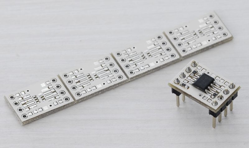
Figure 9
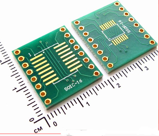
Figure 10
In the next article, I will share some secrets on using solderless breadboards.
Continuation of the article: Useful Tips for Using Solderless Development Boards.
Boris Aladyshkin
See also at bgv.electricianexp.com
: