Categories: Practical Electronics, Novice electricians
Number of views: 100,127
Comments on the article: 2
Logic chips. Part 3
Meet the Digital Chip
In the second part of the article, we talked about the conditional graphic designations of logical elements and about the functions performed by these elements.
To explain the principle of operation, contact circuits performing the logical functions of AND, OR, NOT and AND-NOT were given. Now you can begin to practical acquaintance with the K155 series microcircuits.
Appearance and design
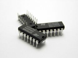
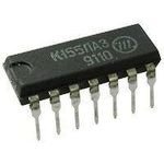 The basic element of the 155th series is the K155LA3 chip. It is a plastic case with 14 leads, on the upper side of which is marked and a key that indicates the first output of the chip.
The key is a small round mark. If you look at the microcircuit from above (from the side of the case), then the conclusions should be counted counterclockwise, and if from below, then clockwise.
A drawing of the case of the microcircuit is shown in Figure 1. Such a case is called DIP-14, which in translation from English means a plastic case with a two-row arrangement of leads. Many microcircuits have a larger number of pins, and therefore the case can be DIP-16, DIP-20, DIP-24 and even DIP-40.
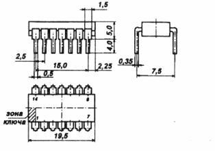
Figure 1. DIP-14 Enclosure.
What is contained in this case
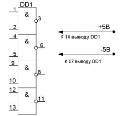
In the DIP-14 package of the K155LA3 microcircuit contains 4 independent elements 2I-NOT. The only thing that unites them is only the general power conclusions: the 14th output of the microcircuit is + the power source, and pin 7 is the negative pole of the source.
In order not to clutter the circuit with unnecessary elements, power lines, as a rule, are not shown. This is also not done because each of the four 2I-NOT elements can be located in different places in the circuit. Usually they simply write on the circuits: “+ 5V lead to conclusions 14 DD1, DD2, DD3 ... DDN. -5V lead to conclusions 07 DD1, DD2, DD3 ... DDN. ". Separately located elements are designated as DD1.1, DD1.2, DD1.3, DD1.4. Figure 2 shows that the K155LA3 chip consists of four 2I-NOT elements. As already mentioned in the second part of the article, input conclusions are located on the left, and outputs on the right.
The foreign analog of K155LA3 is the SN7400 chip and it can be safely used for all the experiments described below. To be more precise, the entire K155 series of chips is an analogue of the foreign SN74 series, so sellers on radio markets offer just that.
Figure 2. The pinout of the K155LA3 chip.
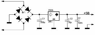
To conduct experiments with a microcircuit, you will need source of power 5V voltage. The easiest way to make such a source is by using the K142EN5A stabilizer microcircuit or its imported version, which is called 7805. At the same time, it is not necessary to wind the transformer, solder the bridge, install capacitors. After all, there will always be some Chinese network adapter with a voltage of 12V, to which it is enough to connect 7805, as shown in Figure 3.
Figure 3. A simple power source for experiments.
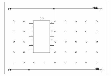
To conduct experiments with the microcircuit, you will need to make a small size breadboard. It is a piece of getinax, fiberglass or other similar insulating material with dimensions of 100 * 70 mm. Even simple plywood or thick cardboard is suitable for such purposes.
Along the long sides of the board, tinned conductors should be strengthened with a thickness of about 1.5 mm, through which power will be supplied to the microcircuits (power buses). Between conductors over the entire area of the breadboard, drill holes with a diameter of not more than 1 mm.
When conducting experiments, it will be possible to insert pieces of tinned wire into them, to which capacitors, resistors and other radio components will be soldered. At the corners of the board, you should make low legs, this will make it possible to place the wires from below.The design of the breadboard is shown in Figure 4.
Figure 4. Development board.
After the breadboard is ready, you can begin to experiment. To do this, at least one K155LA3 chip should be installed on it: solder pins 14 and 7 to the power buses, and bend the remaining pins so that they lie on the board.
Before starting the experiments, you should check the reliability of the soldering, the correct connection of the supply voltage (connecting the supply voltage in the reverse polarity can damage the microcircuit), and also check if there is a short circuit between adjacent terminals. After this check, you can turn on the power and start the experiments.
Best suited for measurements dial voltmeterwhose input impedance is at least 10K / V. Any tester, even cheap Chinese, fully satisfies this requirement.
Why is it better to switch? Because, observing the fluctuations of the arrow, you can notice the voltage pulses, of course a sufficiently low frequency. A digital multimeter does not have this ability. All measurements should be carried out relative to the "minus" of the power source.
After the power is turned on, measure the voltage at all pins of the microcircuit: at the input pins 1 and 2, 4 and 5, 9 and 10, 12 and 13, the voltage should be 1.4V. And at the output terminals 3, 6, 8, 11 about 0.3V. If all voltages are within the specified limits, then the microcircuit is operational.
Figure 5. Simple experiments with a logic element.
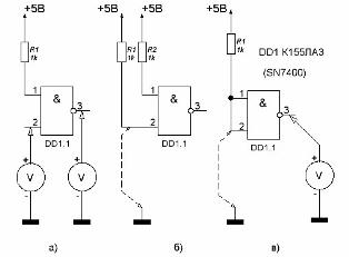
Testing the operation of the logical element 2 AND NOT can be started, for example, from the first element. Its input pins 1 and 2, and output 3. In order to apply a logic zero signal to the input, it is enough to simply connect this input to the negative (common) wire of the power source. If a logical unit is required to be input, then this input should be connected to the + 5V bus, but not directly, but through a limiting resistor with a resistance of 1 ... 1.5 KOhm.
Suppose that we connected input 2 to a common wire, thereby supplying a logic zero to it, and to the input 1 we fed a logical unit, as was just indicated through the terminating resistor R1. This connection is shown in Figure 5a. If, with such a connection, the voltage at the output of the element is measured, then the voltmeter will show 3.5 ... 4.5V, which corresponds to a logical unit. The logical unit will give a measurement of voltage at pin 1.
This completely coincides with what was shown in the second part of the article on the example of the relay-contact circuit 2I-NOT. Based on the results of the measurements, the following conclusion can be made: when one of the inputs of the 2I-NOT element is high and the other is low, the output is sure to have a high level.
Next, we will do the following experiment - we will supply a unit to both inputs at once, as indicated in Figure 5b, but we will connect one of the inputs, for example 2, to a common wire using a wire jumper. (For such purposes, it is best to use a regular sewing needle soldered to flexible wiring). If we now measure the voltage at the output of the element, then, as in the previous case, there will be a logical unit.
Without interrupting the measurements, we remove the wire jumper - the voltmeter will show a high level at the output of the element. This is fully consistent with the logic of the 2I-NOT element, which can be verified by referring to the contact diagram in the second part of the article, as well as by looking at the truth table shown there.
If this jumper is now periodically closed to the common wire of any of the inputs, simulating a low and high level supply, then using a voltmeter the output can detect voltage pulses - the arrow will oscillate in time with the jumper touching the input of the microcircuit.
The following conclusions can be drawn from the experiments: the low-level voltage at the output will appear only when a high level is present at both inputs, that is, condition 2I is satisfied at the inputs.If at least one of the inputs contains a logical zero, the output has a logical unit, we can repeat that the logic of the microcircuit is fully consistent with the logic of the contact circuit 2I-NOT considered in second part of the article.
Here it is appropriate to do one more experiment. Its meaning is to turn off all input pins, just leave them in the “air” and measure the output voltage of the element. What is going to be there? That's right, there will be a logical zero voltage. This suggests that the unconnected inputs of the logic elements are equivalent to the inputs with the logical unit applied to them. You should not forget about this feature, although unused inputs are usually recommended to be connected somewhere.
Figure 5c shows how a 2I-NOT logical element can simply be turned into an inverter. To do this, just connect both of its inputs. (Even if there are four or eight inputs, such a connection is acceptable).
To make sure that the signal at the output has a value opposite to the signal at the input, it is enough to connect the inputs with a wire jumper to a common wire, that is, apply a logic zero to the input. In this case, a voltmeter connected to the output of the element will show a logical unit. If you open the jumper, a low level voltage will appear at the output, which is exactly the opposite of the input voltage.
This experience suggests that the inverter is fully equivalent to the operation of the contact circuit NOT considered in the second part of the article. Such are the generally wonderful properties of the 2I-NOT chip. To answer the question of how all this happens, you should consider the electrical circuit of the 2I-NOT element.
The internal structure of the element 2 is NOT
Until now, we have considered a logical element at the level of its graphic designation, taking it, as they say in mathematics as a “black box”: without going into details of the internal structure of the element, we examined its response to input signals. Now it is time to study the internal structure of our logic element, which is shown in Figure 6.
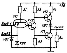
Figure 6. The electrical circuit of the logic element 2I-NOT.
The circuit contains four transistors of the n-p-n structure, three diodes and five resistors. There is a direct connection between transistors (without isolation capacitors), which allows them to work with constant voltages. The output load of the chip is conventionally shown as a resistor Rн. In fact, this is most often the input or several inputs of the same digital circuits.
The first transistor is multi-emitter. It is he who performs the input logical operation 2I, and the following transistors perform the amplification and inversion of the signal. Microcircuits made according to a similar scheme are called transistor-transistor logic, abbreviated as TTL.
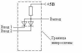
This abbreviation reflects the fact that the input logical operations and the subsequent amplification and inversion are performed by transistor elements of the circuit. In addition to TTL, there is also diode-transistor logic (DTL), the input logical stages of which are performed on diodes located, of course, inside the microcircuit.
Figure 7
At the inputs of the logic element 2I-NOT between the emitters of the input transistor and the common wire, diodes VD1 and VD2 are installed. Their purpose is to protect the input from voltage of negative polarity, which can occur as a result of self-induction of mounting elements when the circuit operates at high frequencies, or simply filed by mistake from external sources.
The input transistor VT1 is connected according to the scheme with a common base, and its load is the transistor VT2, which has two loads. In the emitter, this is the resistor R3, and in the collector R2. Thus, a phase inverter for the output stage on the transistors VT3 and VT4 is obtained, which makes them work in antiphase: when VT3 is closed, VT4 is open and vice versa.
Suppose that both inputs of element 2 AND are NOT low. To do this, simply connect these inputs to a common wire.In this case, the transistor VT1 will be open, which will entail the closure of the transistors VT2 and VT4. The transistor VT3 will be in the open state and through it and the VD3 diode, the current flows into the load - at the output of the element is a high-level state (logical unit).
In that case, if the logic unit is applied to both inputs, the transistor VT1 closes, which will lead to the opening of transistors VT2 and VT4. Due to their opening, the VT3 transistor closes and the current through the load stops. At the output of the element, a zero state or low voltage is set.
The low voltage level is due to a voltage drop at the collector - emitter junction of the VT4 open transistor and, according to specifications, does not exceed 0.4V.
The high level voltage at the output of the element is less than the supply voltage by the magnitude of the voltage drop across the open transistor VT3 and the diode VD3 in the case when the transistor VT4 is closed. High voltage at the output of the element depends on the load, but should not be less than 2.4V.
If a very slowly varying voltage, varying from 0 ... 5V, is applied to the inputs of an element connected together, then it can be seen that the transition of the element from a high level to a low one occurs stepwise. This transition is performed at the moment when the voltage at the inputs reaches a level of approximately 1.2V. Such voltage for the 155th series of microcircuits is called threshold.
This can be considered a general acquaintance with the element 2I-NOT complete. In the next part of the article we will get acquainted with the device of various simple devices, such as various generators and pulse shapers.
Boris Alaldyshkin
Continuation of the article: Logic chips. Part 4
See also at bgv.electricianexp.com
:

