Categories: Practical Electronics, Novice electricians
Number of views: 77535
Comments on the article: 1
Logic chips. Part 2 - Gates
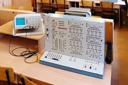 Logical elements operate as independent elements in the form of microcircuits of a small degree of integration, and they are included as components in microcircuits of a higher degree of integration. Such elements can be counted more than a dozen.
But first, we’ll only talk about four of them - these are the elements AND, OR, NOT, AND-NOT. The main elements are the first three, and the AND-NOT element is already a combination of the AND AND NOT elements. These elements can be called "bricks" of digital technology. First you need to consider what is the logic of their action?
Recall the first part of the article on digital circuits. It was said that the voltage at the input (output) of the microcircuit within 0 ... 0.4 V is a logic zero level, or a low voltage level. If the voltage is within 2.4 ... 5.0 V, then this is the level of a logical unit or a high level voltage.
The operating status of K155 series microcircuits and other microcircuits with 5V supply voltage is characterized by precisely such levels. If the voltage at the output of the microcircuit is in the range 0.4 ... 2.4V (for example, 1.5 or 2.0V), then you can already think about replacing this microcircuit.
Practical advice: to make sure that this microcircuit is faulty in output, disconnect the input of the microcircuit following it (or several inputs connected to the output of this microcircuit) from it. These inputs can simply “seat” (overload) the output chip.
Graphic Conventions
Graphic symbols are a rectangle containing input and output lines. Input lines of elements are located on the left, and output lines on the right. The same applies to whole sheets with circuits: on the left side, all signals are input, on the right are outputs. It’s like a line in a book - from left to right, it will be easier to remember. Inside the rectangle is a conditional symbol denoting the function performed by the element.
Logical element AND
We begin the consideration of logical elements with element I.
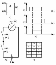
Figure 1. The logical element AND
Its graphic designation is shown in Figure 1a. The symbol of the And function is the English symbol "&", which in English replaces the union "and", because after all, all this "pseudoscience" was invented in the damned bourgeoisie.
The inputs of the element are designated as X with indices 1 and 2, and the output, as an output function, by the letter Y. It is simple, as in school mathematics, for example, Y = K * X or, in the general case, Y = f (x). An element can have more than two inputs, which is limited only by the complexity of the problem being solved, but there can only be one output.
The logic of the element is as follows: a high level voltage at the output Y will be only when And at the input X1 And at the input X2 there will be a high level voltage. If the element has 4 or 8 inputs, then the indicated condition (high level) must be satisfied at all inputs: I-at input 1, I-at input 2, I-at input 3 ... .. And-at input N. Only in this case, the output will also be a high level.
In order to make it easier to understand the logic of the operation of the And element, its analog in the form of a contact circuit is presented in Figure 1b. Here, the output of the element Y is represented by the lamp HL1. If the lamp is lit, then this corresponds to a high level at the output of element I. Often such elements are called 2-I, 3-I, 4-I, 8-I. The first digit indicates the number of inputs.
As input signals X1 and X2, ordinary “bell” buttons are used without fixing. The open state of the buttons is a low level state, and the closed state is naturally high. As a power source, the diagram shows a galvanic battery. While the buttons are in the open state, the lamp, of course, does not shine. The lamp will turn on only when both buttons are pressed at once, i.e. I-SB1, I-SB2.Such is the logical connection between the input and output signal of the element I.
A visual representation of the operation of the AND element can be obtained by looking at the time diagram shown in Figure 1c. At first, a high-level signal appears at input X1, but nothing happened at output Y, there is still a low-level signal. At input X2, the signal appears with some delay relative to the first input, and a high level signal appears at output Y.
When the signal at input X1 is low, the output is also set to low. Or, to put it another way, a high-level signal is held at the output as long as high-level signals are present at both inputs. The same can be said of the more multi-input elements of I: if it is 8-I, then in order to get a high level at the output, the high level must be held at all eight inputs at once.
Most often in the reference literature, the state of the output of logic elements depending on the input signals is given in the form of truth tables. For the considered element 2-I, the truth table is shown in Figure 1d.
The table is somewhat similar to the multiplication table, only smaller. If you study it carefully, you will notice that a high level at the output will be only when a high level voltage or, what is the same thing, a logical unit is present at both inputs. By the way, the comparison of the truth table with the multiplication table is far from accidental: all electronics truth tables know, as they say, by heart.
Also, the function And can be described with algebra of logic or boolean algebra. For a two-input element, the formula will look like this: Y = X1 * X2 or another form of writing Y = X1 ^ X2.
Logical element OR
Next we will look at the OR gate.
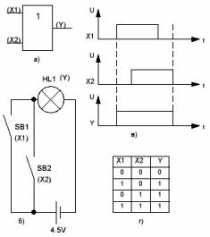
Figure 2. Logic gate OR
Its graphic designation is similar to the AND element just examined, except that instead of the & symbol for the AND function, the number 1 is inscribed inside the rectangle, as shown in Figure 2a. In this case, it denotes the function OR. On the left are the inputs X1 and X2, which, as in the case of the And function, can be more, and on the right the output, indicated by the letter Y.
In the form of a Boolean algebra formula, the OR function is written as Y = X1 + X2.
According to this formula, Y will be true when OR at input X1, OR at input X2, OR at both inputs there will immediately be a high level.
The contact diagram shown in Figure 2b will help to understand what has just been said: pressing either of the buttons (high level) or both buttons at once will cause the lamp to glow (high level). In this case, the buttons are the input signals X1 and X2, and the light is the output signal Y. To make it easier to remember, Figures 2c and 2d show the timing diagram and the truth table, respectively: it is enough to analyze the operation of the shown contact circuit with the diagram and table, as all questions will disappear.
Logic element NOT, inverter
As one teacher said, in digital technology there is nothing more complicated than an inverter. Perhaps this is in fact.
In the algebra of logic, the operation is NOT called inversion, which means negation in English, that is, the signal level at the output corresponds exactly the opposite to the input signal, which looks like Y = / X in the form of a formula
(The slash before X denotes the actual inversion. Usually, the underscore is used instead of the slash, although this notation is quite acceptable.).
The graphic symbol of the element is NOT a square or rectangle inside which the number 1 is inscribed.
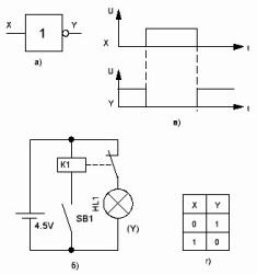
Figure 3. Inverter
In this case, it means that this element is an inverter. It has only one input X and output Y. The output line begins with a small circle, which actually indicates that this element is an inverter.
As just said, an inverter is the most complex digital circuitry.And this is confirmed by his contact scheme: if before that only buttons were enough, now a relay has been added to them. While the SB1 button is not pressed (logical zero at the input), relay K1 is de-energized and its normally-closed contacts turn on the HL1 bulb, which corresponds to a logical unit at the output.
If you press the button (apply a logical unit to the input), the relay will turn on, the K1.1 contacts will open, the light will go out, which corresponds to a logical zero at the output. The above is confirmed by the time diagram in Figure 3c and the truth table in Figure 3d.
Logical element AND NOT
The AND gate is NOT a combination of the AND gate and the NOT gate.
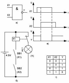
Figure 4. The logical element AND NOT
Therefore, the symbol & (logical AND) is present on its graphic symbol, and the exit line starts with a circle indicating the presence of an inverter element.
The contact analog of the logic element is shown in Figure 4b, and, if you look closely, it is very similar to the analog of the inverter shown in Figure 3b: the bulb is also turned on through the normally-closed contacts of relay K1. Actually this is the inverter. The relay is controlled by buttons SB1 and SB2, which correspond to the inputs X1 and X2 of the AND gate. The diagram shows that the relay will be turned on only when both buttons are pressed: in this case, the buttons perform the & function (logical AND). In this case, the lamp at the output goes out, which corresponds to the state of logical zero.
If both buttons are not pressed, or at least one of them, then the relay is disabled, and the light at the output of the circuit is on, which corresponds to the level of a logical unit.
From the foregoing, we can draw the following conclusions:
Firstly, if at least one input has a logical zero, then the output will be a logical unit. The same state at the output will be in the case when zeros are present at both inputs at once. This is a very valuable property of AND-NOT elements: if you connect both inputs, then the AND-NOT element becomes an inverter - it simply performs the function of NOT. This property allows you not to put a special chip containing six inverters at once, when only one or two are required.
Secondly, zero at the output can be obtained only if "collect" on all inputs of unity. In this case, it would be appropriate to name the considered logical element 2I-NOT. The two says that this element is two-input. In almost all series of microcircuits, there are also 3, 4 and eight-input elements. Moreover, each of them has only one way out. However, the 2I-NOT element is considered a basic element in many series of digital microcircuits.
With various options for connecting the inputs, you can get another wonderful property. For example, connecting the three inputs of the eight-input element 8I-NOT together, we get the element 6I-NOT. And if you connect all 8 inputs together, you get just an inverter, as mentioned above.
This completes the acquaintance with the logical elements. In the next part of the article, we will consider the simplest experiments with microcircuits, the internal structure of microcircuits, simple devices, such as pulse generators.
Boris Aladyshkin
Continuation of the article: Logic chips. Part 3
See also at bgv.electricianexp.com
:

