Categories: Featured Articles » Practical Electronics
Number of views: 12919
Comments on the article: 0
Chip 4046 (K564GG1) for devices with resonance retention - the principle of operation
When creating a power electronic device with resonance retention in the LC circuit, a resonant controller circuit is designed to synchronize the received oscillations with control pulses coming from the driver.
The task of this controller is to keep resonant oscillations in the LC circuit by exciting it in time with its own oscillations. To achieve this, the controller needs to receive a signal from the loop from the circuit containing data on the current frequency and phase of free oscillations in it, after which, relying on these data, maintain the driver stage in synchronization with these frequency and phase, then the resonance in the circuit will be automatically saved.
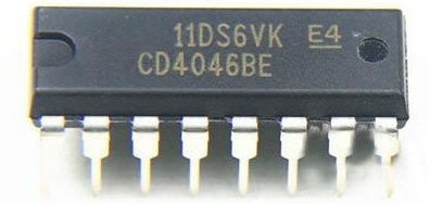
To build such a controller, the CD4046 chip or its domestic counterpart K564GG1 is suitable. Let's look at the device of this microcircuit, the purpose of its conclusions and the connection diagram of the mounted components, in order to understand what you are dealing with if necessary.
This chip allows you to easily organize a PLL - phase-locked loop. To build a PLL, three necessary blocks are used that are located inside the microcircuit: a VCO - voltage controlled oscillator, a FC - phase comparator, and an LPF - low-pass filter.
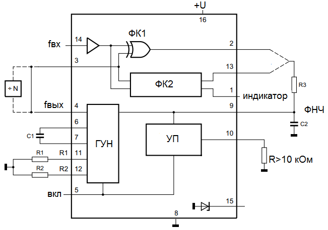
Built-in to the microcircuit, the VCO generates a sequence of rectangular pulses with 50% coverage, that is, a pure meander whose initial frequency depends on the parameters of two RC circuits: R1C1 and R2C2 connected to it outside the microcircuit, and the amplitude in this case is close to the supply voltage of the microcircuit U +.
PLL principle of operation
The external input signal fin is supplied to the microcircuit, in fact, to one of the inputs of the phase comparator FC (FC1 or FC2 - the developer selects) inside it. A meander produced by the VCO is simultaneously fed to the second FC input. As a result, a rectangular signal is obtained at the FC output, the pulse duration in which depends on the difference between the pulses from the VCO and the external pulses at each moment of time.
In fact, the duration of the output pulses with the FC is proportional to the phase difference of the two compared signals. The fact is that the exclusive-OR logic element is often used as a FC, this means that at the FC output there will be a high voltage level only if there is a difference between the signals, and if there is no difference then the output from the FC will be low voltage level or inactive state.

From the output of the FC, the signal is fed to a low-pass filter, which is a simple RC circuit, on the capacitor of which a pulsating mismatch voltage is obtained, the ripple level being proportional to the difference of the two signals (from the internal VCO and supplied to the microcircuit from the outside), in fact - the phase difference .
The mismatch voltage obtained at the LPF capacitor is immediately fed back to the VCO input, and depending on its average value, the VCO frequency will be automatically tuned so that the frequency of the meander at its output fout approaches the frequency of the external signal coming from the outside of the microcircuit. Upon reaching such a situation, the average voltage across the capacitor of the low-pass filter will be the smallest - this is a sign of the maximum convergence of the two signals in frequency and phase. When the signal is thus captured, it will continue to be held by the PLL loop.
The limits of the reorganization of the VCO
As you already understood, the VCO frequency is capable of tuning within a certain range of auto-tuning. This range is set by the external components of the chip. And the reaction speed of the PLL system is determined by the time constant of the LFF (values C2 and R3).For this reason, you should strictly approach the choice of mounted components of the chip.
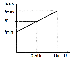
The supply voltage of the microcircuit, the capacitor C1, as well as the resistors R1 and R2 determine the VCO frequency self-tuning range inside the microcircuit. Resistor R2 biases the minimum frequency fmin of the VCO above zero. And the ratio between the values of the resistors R1 and R2 determines the ratio between the maximum and minimum frequencies - fmax / fmin, tunable output signal from the VCO.
Chip inputs and outputs
Conclusion 4 - signal output of the VCO, on it in the working mode the meander. This output can be used to supply a signal to other blocks of the designed device.
Pin 5 is responsible for turning the VCO on and off. When a high level voltage is applied to this output, the microcircuit will turn off. When applying a low voltage level (when connecting pin 5 to the common wire) - the microcircuit will work in normal mode.
Conclusions 6 and 7. The capacitor C1 is connected to them - this is the frequency-setting capacitor of the VCO.
Conclusion 8 - the common power wire of the chip.
Resistor R1 is between terminal 11 and the common wire. Resistor R2 - between terminal 12 and the common wire. These are frequency setting resistors. Resistor R3 of the low-pass filter - to pin 9 and pin 2 or 13 (the difference between them will be discussed later), the capacitor C2 of the low-pass filter is between pin 9 and the common wire.
Pin 10 is the output of the repeater amplifier. The voltage on it during the operation of the microcircuit is the mismatch voltage supplied to the low-pass filter. Conclusion 10 is designed so that the mismatch voltage can, if necessary, be easily isolated without shunting the LPF capacitor. To this conclusion, it is allowed to connect a resistor with a resistance of more than 10 kOhm.
Conclusion 15 - on it is the cathode of the built-in zener diode with a stabilization voltage of 5.6 volts (the stabilization voltage of this zener diode may be different, depending on the manufacturer of the chip). This zener diode can optionally be used in the power circuit of the chip.
Conclusion 16 - plus the power of the chip.
Inputs and outputs of phase comparators FC1 and FC2
The meander from the output of the VCO is taken from terminal 4 and fed to terminal 3, connected through an amplifier-shaper to the inputs of the phase comparators FC1 and FC2. If desired, the signal from the VCO can be optionally passed through a frequency divider.
Input 14 is a signal input, and an input signal is fed to it, with which it is necessary to synchronize the output signal at the output of the VCO. Depending on the nature of the input signal, the developer can choose which of the phase comparators to use: FC1 or FC2, and attach a low-pass filter resistor to the selected comparator (to pin 2 or 13). The phase comparator FC2 has an indicator pin 1, a high level voltage appears on it when the signals are maximally synchronized.
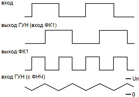
A feature of FC1 is that it is a simple exclusive-OR logic element, and the quality of its operation depends on the parameters of the low-pass filter at its output. Work begins with the center frequency f0 = (fmax-fmin) / 2, it is possible to capture the harmonics of the center frequency. It has high noise immunity.
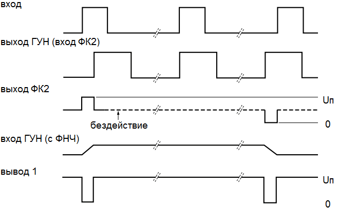
The peculiarity of FC2 is that it processes only the positive differences of the pulses supplied to it, and therefore the duty cycle of the pulses therefore does not matter. The work starts with the minimum frequency fmin, there is no possibility of capturing the harmonics of the central frequency. It has low noise immunity. In the low-pass filter, a capacitor with a low leakage current is required. FC2 is better suited for use in power circuits with LC resonance.
Selection of attachments
As a low-pass filter of the low-pass filter, a resistor R3 and a capacitor C2 are installed. For the PLL to work correctly, the RC time constant must be ten times greater than the approximate PLL capture frequency.
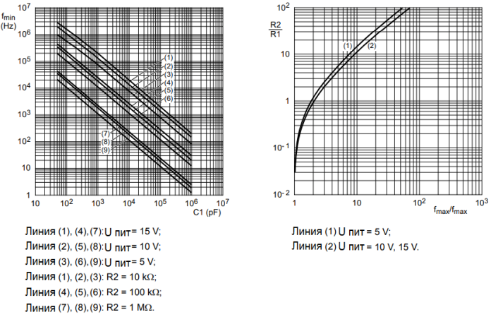
As a rule, the capture frequency is approximately known to the developer, therefore, they are initially set by the frequency auto-tuning range: fmin and fmax. The first nomogram determines, taking into account the supply voltage of the microcircuit and the required fmin, the values of R2 and C1.Then, according to the second nomogram, based on the required ratio fmax / fmin, R1 is selected. It is better to provide the ability to adjust the resistors in the circuit.
See also at bgv.electricianexp.com
:
