Categories: Featured Articles » Practical Electronics
Number of views: 174,150
Comments on the article: 6
Field effect transistors: principle of operation, circuits, operating modes and modeling
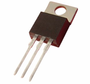
We have already reviewed device of bipolar transistors and their workNow let's find out what field effect transistors are. Field effect transistors are very common in both old circuitry and modern. Nowadays, devices with an insulated gate are used to a greater extent, we will talk about the types of field-effect transistors and their features today. In the article, I will make comparisons with bipolar transistors in separate places.
Definition
A field effect transistor is a semiconductor fully controllable key controlled by an electric field. This is the main difference from the point of view of practice from bipolar transistors, which are controlled by current. An electric field is created by a voltage applied to the gate relative to the source. The polarity of the control voltage depends on the type of transistor channel. There is a good analogy with electronic vacuum tubes.
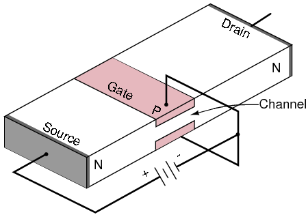
Another name for field effect transistors is unipolar. "UNO" means one. In field-effect transistors, depending on the type of channel, the current is carried out by only one type of carrier by holes or electrons. In bipolar transistors, the current was formed from two types of charge carriers - electrons and holes, regardless of the type of devices. Field effect transistors in the general case can be divided into:
-
transistors with a control pn junction;
-
insulated gate transistors.
Both of them can be n-channel and p-channel, a positive control voltage must be applied to the gate of the former to open the key, and for the latter, negative with respect to the source.
All types of field-effect transistors have three outputs (sometimes 4, but rarely, I met only in Soviet and it was connected to the case).
1. Source (carrier source, bipolar emitter analog).
2. Stoke (a source of charge carriers from the source, an analog of the collector of a bipolar transistor).
3. Shutter (control electrode, analog of a grid on lamps and bases on bipolar transistors).
PN Transistor Transistor
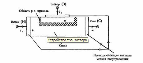
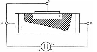
The transistor consists of the following areas:
1. Channel;
2. Stock;
3. The source;
4. Shutter.
In the image you see a schematic structure of such a transistor, the findings are connected to the metallized sections of the gate, source and drain. In a specific circuit (this is a p-channel device), the gate is an n-layer, has less resistivity than the channel region (p-layer), and the p-n junction region is more located in the p-region for this reason.
Conditional graphic designation:

a - field-effect transistor n-type, b - field-effect transistor p-type
To make it easier to remember, remember the designation of the diode, where the arrow points from the p-region to the n-region. Here also.
The first state is to apply external voltage.
If voltage is applied to such a transistor, plus to the drain, and minus to the source, a large current flows through it, it will be limited only by the channel resistance, external resistances and internal resistance of the power source. You can draw an analogy with a normally closed key. This current is called Istart or the initial drain current at Us = 0.
A field effect transistor with a pn junction control, without the applied control voltage to the gate, is as open as possible.
The voltage to the drain and source is applied in this way:
The main charge carriers are introduced through the source!
This means that if the transistor is p-channel, then the positive output of the power source is connected to the source, because the main carriers are holes (positive charge carriers) - this is the so-called hole conductivity.If the n-channel transistor is connected to the source, the negative output of the power source, because in it, the main charge carriers are electrons (negative charge carriers).
The source is the source of the main charge carriers.
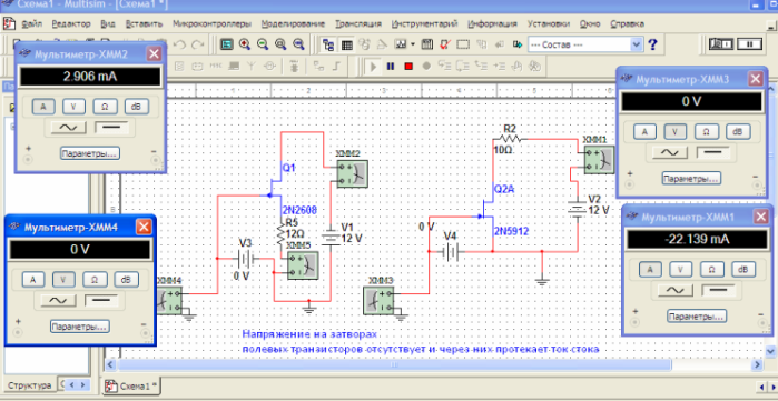
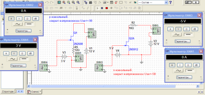
Here are the results of modeling such a situation. On the left is a p-channel, and on the right is an n-channel transistor.
The second state - apply voltage to the shutter
When a positive voltage is applied to the gate relative to the source (Us) for the p-channel and negative for the n-channel, it shifts in the opposite direction, the p-n junction region expands towards the channel. As a result of which the channel width decreases, the current decreases. The gate voltage at which the current through the key stops flowing is called the cut-off voltage.
The key begins to close.

The cut-off voltage is reached and the key is completely closed. The picture with the simulation results shows such a state for the p-channel (left) and n-channel (right) keys. By the way, in English such a transistor is called JFET.
Operating modes
The operating mode of the transistor with a voltage Uзи is either zero or reverse. Due to the reverse voltage, you can "cover the transistor", used in class A amplifiers and other circuits where smooth regulation is needed.
The cutoff mode occurs when Uzi = U cutoff for each transistor it is different, but in any case it is applied in the opposite direction.
Characteristics, CVC
An output characteristic is a graph that depicts the dependence of the drain current on Uci (applied to the terminals of the drain and source) at various gate voltages.
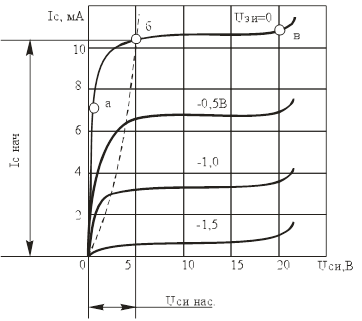
Can be divided into three areas. At the beginning (on the left side of the graph) we see the ohmic region - in this interval the transistor behaves like a resistor, the current increases almost linearly, reaching a certain level, goes into the saturation region (in the center of the graph).
In the right part of the graph we see that the current begins to grow again, this is the breakdown region, here the transistor should not be located. The uppermost branch shown in the figure is the current at zero Us, we see that the current here is the largest.
The higher the voltage Uzi, the lower the drain current. Each of the branches differs by 0.5 volts at the gate. What we confirmed by modeling.
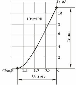
The drain-gate characteristic, i.e. dependence of the drain current on the gate voltage at the same drain-source voltage (in this example 10V), here the grid pitch is also 0.5V, we again see that the closer the voltage Uzi is to 0, the larger the drain current.
In bipolar transistors, there was such a parameter as the current transfer coefficient or gain, it was denoted as B or H21e or Hfe. In the field, the steepness is used to display the ability to increase voltage. It is indicated by the letter S
S = dIc / dU
That is, the steepness shows how much milliamps (or amperes) the drain current grows with an increase in the gate-source voltage by the number of volts with an unchanged drain-source voltage. It can be calculated on the basis of the gate-gate characteristic; in the above example, the slope is about 8 mA / V.
Switching schemes
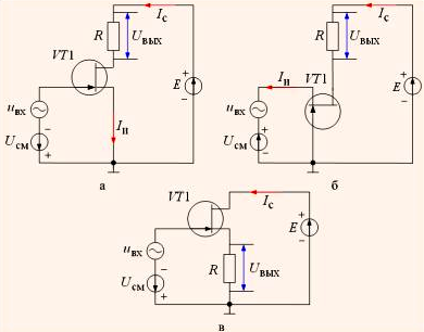
Like bipolar transistors, there are three typical wiring diagrams:
1. With a common source (a). It is used most often, gives gain in current and power.
2. With a common shutter (b). Rarely used, low input impedance, no gain.
3. With a total drain (c). The voltage gain is close to 1, the input impedance is large, and the output impedance is low. Another name is a source follower.
Features, advantages, disadvantages
-
The main advantage of the field effect transistor high input impedance. Input resistance is the ratio of current to gate-source voltage. The principle of operation lies in the control using an electric field, and it is formed when voltage is applied. I.e field effect transistors.
-
Field-effect transistor practically does not consume control current, this is reduces control loss, signal distortion, current overload of the signal source ...
-
Average frequency Field-effect transistors perform better than bipolar, this is due to the fact that less time is required for the "resorption" of charge carriers in the areas of a bipolar transistor. Some modern bipolar transistors can even surpass field ones, this is due to the use of more advanced technologies, reducing the width of the base, and more.
-
The low noise level of field-effect transistors is due to the absence of a charge injection process, as in bipolar ones.
-
Stability with temperature.
-
Low power consumption in the conductive state - greater efficiency of your devices.
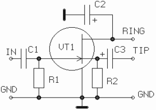
The simplest example of using high input impedance is matching devices for connecting electro-acoustic guitars with piezo pickups and electric guitars with electromagnetic pickups to line inputs with low input impedance.
A low input impedance can cause a drop in the input signal, distorting its shape to varying degrees depending on the frequency of the signal. This means that you need to avoid this by introducing a cascade with a high input impedance. Here is the simplest diagram of such a device. Suitable for connecting electric guitars to the line input of the computer's audio card. With it, the sound will become brighter, and the timbre will be richer.
The main disadvantage is that such transistors are afraid of static. You can take an element with your electrified hands and it will immediately fail, this is a consequence of managing the key using the field. They are recommended to work with them in dielectric gloves, connected through a special bracelet to ground, with a low-voltage soldering iron with an insulated tip, and the transistor leads can be tied with wire to short-circuit them during installation.
Modern devices are practically not afraid of this, because at the entrance to them protective devices such as zener diodes can be built in, which operate when the voltage is exceeded.
Sometimes, for beginner radio amateurs, fears reach the point of absurdity, such as putting foil caps on the head. Everything described above, although it is mandatory, but not observing any conditions does not guarantee the failure of the device.
Insulated Gate Field Effect Transistors
This type of transistor is actively used as a semiconductor controlled key. Moreover, they work most often in the key mode (two positions “on” and “off”). They have several names:
1. MOS transistor (metal-dielectric-semiconductor).
2. MOS transistor (metal oxide semiconductor).
3. MOSFET transistor (metal-oxide-semiconductor).
Remember - these are just variations of the same name. The dielectric, or as it is also called oxide, plays the role of an insulator for the gate. In the diagram below, an insulator is shown between the n-region near the shutter and the shutter in the form of a white zone with dots. It is made of silicon dioxide.
The dielectric eliminates electrical contact between the gate electrode and the substrate. Unlike the control pn junction, it does not work on the principle of expanding the transition and channel overlap, but on the principle of changing the concentration of charge carriers in the semiconductor under the influence of an external electric field. MOSFETs are of two types:
1. With integrated channel.
2. With induced channel
Channel Integrated Transistors
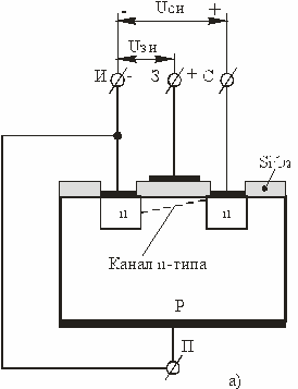
In the diagram you see a transistor with an integrated channel. One can already guess from it that the principle of its operation resembles a field-effect transistor with a control p-n junction, i.e. when the gate voltage is zero, current flows through the switch.
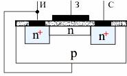
Near the source and sink, two regions with a high content of impurity charge carriers (n +) with increased conductivity are created. A substrate is a P-type base (in this case).
Please note that the crystal (substrate) is connected to the source, it is drawn on many conventional graphic symbols.When the gate voltage increases, a transverse electric field arises in the channel, it repels charge carriers (electrons), and the channel closes when the threshold value Uz is reached.
Operating modes
When a negative gate-source voltage is applied, the drain current drops, the transistor starts to close - this is called the lean mode.
When a positive voltage is applied to the gate-source, the reverse process occurs - the electrons are attracted, the current increases. This is an enrichment mode.
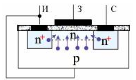
All of the above is true for MOS transistors with an integrated N-type channel. If the p-type channel replaces all the words “electrons” with “holes”, the polarity of the voltage is reversed.
Modeling
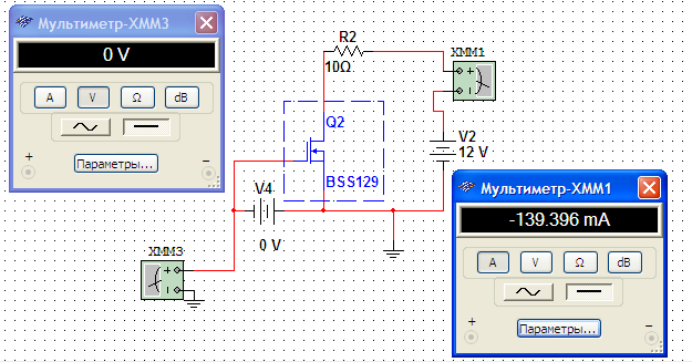
Transistor with built-in n-type channel with zero gate voltage:
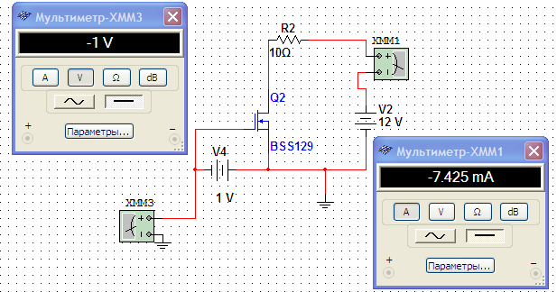
We apply -1V to the shutter. Current decreased by 20 times.
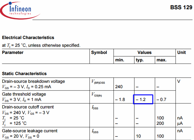
According to the datasheet for this transistor, we have a threshold gate-source voltage in the region of one volt, and its typical value is 1.2 V, check this.
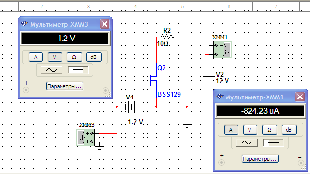
The current has become in microamperes. If you increase the voltage a little more, it will disappear completely.

I chose a transistor at random, and I came across a fairly sensitive device. I'll try to change the polarity of the voltage so that the gate has a positive potential, we will check the enrichment mode.
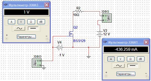
At a gate voltage of 1 V, the current increased four times, compared with what it was at 0 V (first picture in this section). It follows that, unlike the previous type of transistors and bipolar transistors, it can work both to increase the current and to decrease without additional strapping. This statement is very rude, but in a first approximation has a right to exist.
Specifications
Here, everything is almost the same as in a transistor with a control transition, except for the presence of an enrichment mode in the output characteristic.
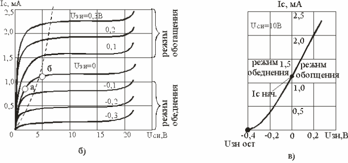
On the drain-gate characteristic, it is clearly seen that a negative voltage causes the mode of depletion and closure of the key, and a positive voltage at the gate causes enrichment and greater opening of the key.
Channel Induced Transistors
MOSFETs with an induced channel do not conduct current when there is no voltage on the gate, or rather, there is current, but it is extremely small, because this is the return current between the substrate and the high-alloyed areas of the drain and source.
Field-effect transistor with an isolated gate and an induced channel is an analog of a normally-open switch, current does not flow.
In the presence of a gate-source voltage, as we consider the n-type of the induced channel, the voltage is positive, negative carriers are attracted to the gate region by the action of the field.
So there is a “corridor” for electrons from source to drain, so a channel appears, the transistor opens, and current begins to flow through it. We have a p-type substrate, the main ones in it are positive charge carriers (holes), there are very few negative carriers, but under the influence of the field they detach from their atoms and their movement begins. Hence the lack of conductivity in the absence of voltage.
Specifications
The output characteristic exactly repeats the same difference from the previous ones, only that the voltages Uz become positive.
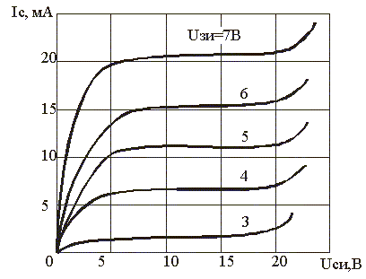
The close-gate characteristic shows the same thing, the differences again in the gate voltages.
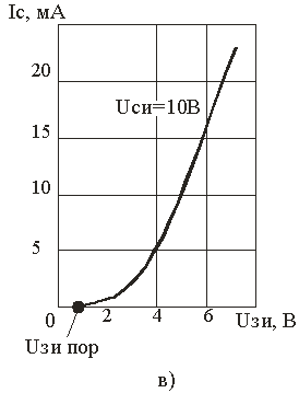
When considering the current-voltage characteristics, it is extremely important to carefully look at the values written along the axes.
Modeling
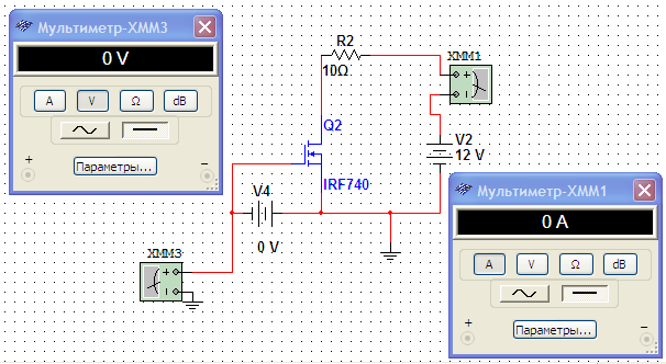
A voltage of 12 V was applied to the key, and we had 0. At the gate, current does not flow through the transistor.
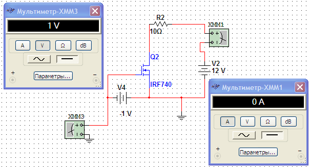
Add 1 volt to the gate, but the current did not think to flow ...
Adding one volt, I found that the current begins to grow from 4v.

Adding another 1 Volt, the current increased sharply to 1.129 A.
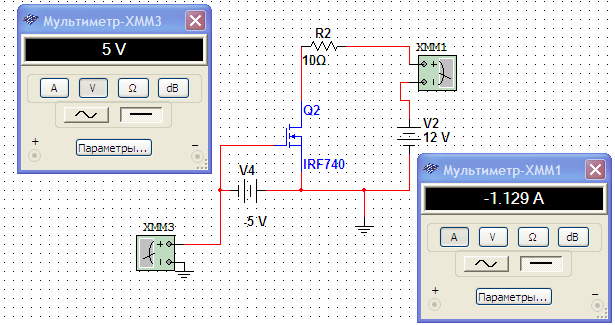
The Datasheet indicates the threshold voltage for opening this transistor in a section from 2 to 4 volts, and the maximum on a gate-to-gate from -20 to +20 V, further voltage increments did not give results at 20 volts (several milliamperes I did not I think in this case).
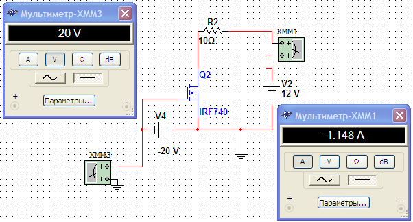
This means that the transistor would be completely open, if it weren’t, the current in this circuit would be 12/10 = 1.2 A. Later I studied how this transistor works, and found out that at 4 volts it starts to open.
Adding 0.1V each, I noticed that with every tenth of a volt, the current grows more and more, and by 4.6 volts the transistor is almost completely open, the difference with the gate voltage of 20V in the drain current is only 41 mA, at 1.1 A it nonsense.
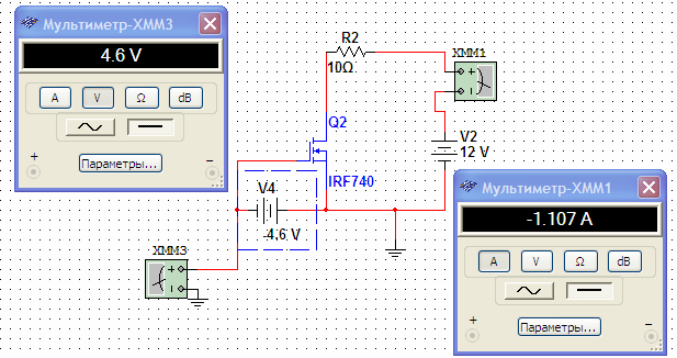
This experiment reflects the fact that the transistor with an induced channel opens only when the threshold voltage is reached, which allows it to work perfectly as a key in pulse circuits. Actually, IRF740 is one of the most common in switching power supplies.
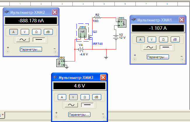
The results of measurements of the gate current showed that field-effect transistors almost do not consume control current. At a voltage of 4.6 volts, the current was only 888 nA (nano !!!).
At a voltage of 20V, it was 3.55 μA (micro). For a bipolar transistor, it would be on the order of 10 mA, depending on the gain, which is tens of thousands of times more than a field one.
Not all keys are opened by such voltages, this is due to the design and features of the circuitry of the devices where they are used.
Features of using keys with an insulated shutter
Two conductors, and between them a dielectric - what is it? This is a transistor, the gate itself has a parasitic capacitance, it slows down the process of switching the transistor. This is called the Miller Plateau, in general, this question is worthy of a separate serious material with accurate modeling, using other software (did not check this feature in multisim).
A discharged capacity at the first moment of time requires a large charging current, and rare control devices (PWM controllers and microcontrollers) have strong outputs, so they use drivers for field shutters, both in field effect transistors and in IGBT (bipolar with an isolated shutter). This is such an amplifier that converts the input signal into an output of such magnitude and current strength, sufficient to turn the transistor on and off. The charge current is also limited by a resistor connected in series with the gate.
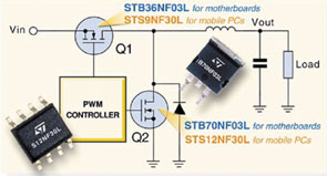
At the same time, some gates can be controlled from the microcontroller port through a resistor (the same IRF740). We touched on this topic. in the arduino material cycle.
Conditional Graphics
They resemble field-effect transistors with a control gate, but differ in that on the UGO, as in the transistor itself, the gate is separated from the substrate, and the arrow in the center indicates the type of channel, but is directed from the substrate to the channel, if it is an n-channel mosfet - towards the shutter and vice versa.
For keys with induced channel:
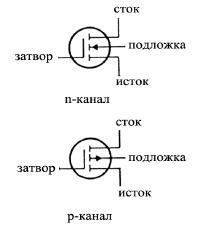
It might look like this:
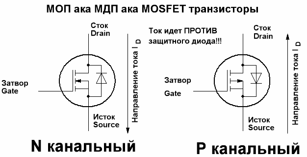
Pay attention to the English names of the conclusions, they are often indicated on the datasheet’s and on the diagrams.
For keys with a built-in channel:
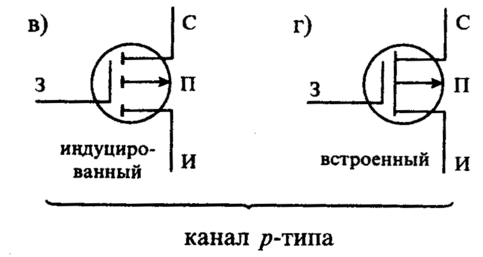
See also at bgv.electricianexp.com
:
