Categories: Featured Articles » Practical Electronics
Number of views: 151627
Comments on the article: 0
DC-DC Converters
To power various electronic equipment, DC / DC converters are very widely used. They are used in computing devices, communication devices, various control and automation circuits, etc.
Transformer power supplies
In traditional transformer power supplies, the voltage of the mains is converted by a transformer, most often lowered, to the desired value. Undervoltage rectified by a diode bridge and smoothed by a capacitor filter. If necessary, a semiconductor stabilizer is placed after the rectifier.
Transformer power supplies are usually equipped with linear stabilizers. There are at least two advantages of such stabilizers: it is a small cost and a small number of parts in the harness. But these advantages are consumed by low efficiency, since a significant part of the input voltage is used to heat the control transistor, which is completely unacceptable for powering portable electronic devices.
DC / DC Converters
If the equipment is powered by galvanic cells or batteries, then voltage conversion to the desired level is possible only with the help of DC / DC converters.
The idea is quite simple: a constant voltage is converted to alternating voltage, as a rule, with a frequency of several tens or even hundreds of kilohertz, it rises (decreases), and then it is rectified and fed to the load. Such converters are often called pulse.
An example is the boost converter from 1.5V to 5V, just the output voltage of a computer USB. A similar power converter is sold on Aliexpress.
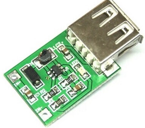
Fig. 1. 1.5V / 5V converter
Pulse converters are good in that they have high efficiency, within 60..90%. Another advantage of pulse converters is a wide range of input voltages: the input voltage can be lower than the output voltage or much higher. In general, DC / DC converters can be divided into several groups.
Classification of converters
Step-down or buck
The output voltage of these converters, as a rule, is lower than the input: without special losses for heating the control transistor, you can get a voltage of only a few volts at an input voltage of 12 ... 50V. The output current of such converters depends on the demand of the load, which in turn determines the circuitry of the converter.
Another English name for the chopper buck converter. One of the options for translating this word is a breaker. In the technical literature, the buck converter is sometimes called a “chopper”. For now, just remember this term.
Step-up or boost in English terminology
The output voltage of these converters is higher than the input. For example, with an input voltage of 5V, an output of up to 30V can be obtained; moreover, it can be continuously regulated and stabilized. Boost converters are often called boosters.
Universal Converters - SEPIC
The output voltage of these converters is held at a predetermined level with an input voltage both higher than the input and lower. It is recommended in cases where the input voltage can vary significantly. For example, in a car, the battery voltage can vary between 9 ... 14V, and you need to get a stable voltage of 12V.
Inverting converters - inverting converter
The main function of these converters is to obtain the output voltage of reverse polarity relative to the power source. Very convenient in cases where bipolar nutrition is required, for example to power the op-amp.
All of these converters can be stabilized or unstabilized, the output voltage can be galvanically connected to the input or have galvanic isolation of voltages. It all depends on the specific device in which the converter will be used.
In order to proceed to the further discussion of DC / DC converters, one should at least deal with the theory.
Chopper down converter - buck type converter
Its functional diagram is shown in the figure below. The arrows on the wires indicate the direction of the currents.
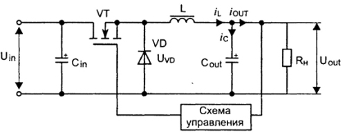
Fig. 2. Functional diagram of chopper stabilizer
The input voltage Uin is applied to the input filter - capacitor Cin. The VT transistor is used as a key element; it carries out high-frequency current switching. It could be MOSFET structure transistor, IGBT or conventional bipolar transistor. In addition to these details, the circuit contains a discharge diode VD and an output filter - LCout, from which the voltage enters the load Rн.
It is easy to see that the load is connected in series with the elements VT and L. Therefore, the circuit is consistent. How does undervoltage occur?
Pulse Width Modulation - PWM
The control circuit generates rectangular pulses with a constant frequency or constant period, which is essentially the same thing. These pulses are shown in Figure 3.
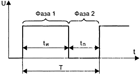
Fig. 3. Control pulses
Here t is the pulse time, the transistor is open, tp is the pause time, and the transistor is closed. The ti / T ratio is called the duty cycle duty cycle, denoted by the letter D and is expressed in %% or simply in numbers. For example, with D equal to 50%, it turns out that D = 0.5.
Thus, D can vary from 0 to 1. With a value of D = 1, the key transistor is in a state of full conductivity, and at D = 0 in a cut-off state, simply speaking, it is closed. It is easy to guess that at D = 50% the output voltage will be equal to half the input.
It is quite obvious that the regulation of the output voltage occurs due to a change in the width of the control pulse t and, in fact, a change in the coefficient D. This principle of regulation is called pulse width modulated PWM (PWM). In almost all switching power supplies, it is precisely with the help of PWM that the output voltage is stabilized.
In the diagrams shown in Figures 2 and 6, the PWM is “hidden” in the rectangles with the inscription “Control circuit”, which performs some additional functions. For example, it can be a smooth start of the output voltage, remote switching on or protection of the converter against short circuit.
In general, converters were so widely used that companies producing electronic components arranged for PWM controllers for all occasions. The range is so large that just to list them you will need a whole book. Therefore, it does not occur to anyone to assemble converters on discrete elements, or as they often say on "loose powder".
Moreover, ready-made converters of small capacity can be bought at Aliexpress or Ebay for a small price. At the same time, for installation in an amateurish design, it is enough to solder the input and output wires to the board, and set the required output voltage.
But back to our figure 3. In this case, the coefficient D determines how much time will be open (phase 1) or closed (phase 2) key transistor. For these two phases, you can imagine the diagram in two figures. The figures DO NOT SHOW those elements that are not used in this phase.
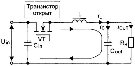
Fig. 4. Phase 1
When the transistor is open, the current from the power source (galvanic cell, battery, rectifier) passes through an inductive choke L, a load Rн, and a charging capacitor Cout. In this case, a current flows through the load, the capacitor Cout and inductor L accumulate energy. Current iL gradually increases, the effect of the inductance of the inductor affects. This phase is called pumping.
After the voltage at the load reaches the set value (determined by the control device settings), the transistor VT closes and the device moves to the second phase - the discharge phase. The closed transistor in the figure is not shown at all, as if it did not exist. But this only means that the transistor is closed.
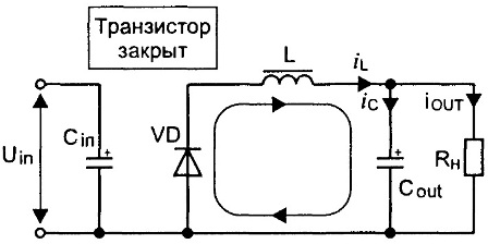
Fig. 5. Phase 2
When the transistor VT is closed, there is no replenishment of energy in the inductor, since the power source is disconnected. Inductance L tends to prevent a change in the magnitude and direction of the current (self-induction) flowing through the inductor winding.
Therefore, the current cannot stop instantly and closes through the diode-load circuit. Because of this, the VD diode is called bit. As a rule, this is a high-speed Schottky diode. After the control period of phase 2, the circuit switches to phase 1, the process is repeated again. The maximum voltage at the output of the considered circuit can be equal to the input, and no more. To obtain an output voltage greater than the input voltage, boost converters are used.
It should be noted that in fact, not everything is as simple as written above: it is assumed that all components are perfect, i.e. switching on and off occurs without delay, and the active resistance is zero. In the practical manufacture of such schemes, many nuances have to be taken into account, since a lot depends on the quality of the components used and the parasitic capacitance of the installation. Only about such a simple detail as a throttle (well, just a coil of wire!), You can write more than one article.
For now, it is only necessary to recall the inductance value itself, which determines two chopper operating modes. With insufficient inductance, the converter will operate in discontinuous current mode, which is completely unacceptable for power sources.
If the inductance is large enough, then the work takes place in the continuous current mode, which allows using the output filters to obtain a constant voltage with an acceptable level of ripple. In the continuous current mode, step-up converters also work, which will be described below.
For some increase in efficiency, the VD discharge diode is replaced by a MOSFET transistor, which is opened at the right time by the control circuit. Such converters are called synchronous. Their use is justified if the power of the converter is large enough.
Step-up or boost boost converters
Boost converters are mainly used for low-voltage power supply, for example, from two to three batteries, and some components require 12 ... 15 V with low current consumption. Quite often, the boost converter is briefly and clearly called the word “booster”.
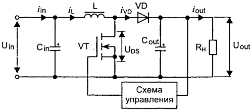
Fig. 6. Functional diagram of boost converter
The input voltage Uin is applied to the input filter Cin and applied to the series-connected inductor L and switching transistor VT. A diode VD is connected to the connection point of the coil and drain of the transistor. A load Rн and a shunt capacitor Cout are connected to the other terminal of the diode.
The transistor VT is controlled by a control circuit that generates a stable frequency control signal with an adjustable duty cycle D, in the same way as described above in the description of the chopper circuit (Fig. 3). The VD diode at the right time blocks the load from the key transistor.
When the key transistor is open, the right-side output of the coil L is connected to the negative pole of the power supply Uin. Rising current (the effect of inductance affects) from the power source flows through the coil and an open transistor, energy is accumulated in the coil.
At this time, the VD diode blocks the load and the output capacitor from the key circuit, thereby preventing the discharge of the output capacitor through an open transistor. The load at this moment is powered by the energy stored in the capacitor Cout. Naturally, the voltage across the output capacitor drops.
As soon as the output voltage becomes slightly lower than the set value (determined by the control circuit settings), the key transistor VT closes, and the energy stored in the inductor recharges the capacitor Cout through the diode VD, which feeds the load. In this case, the self-induction EMF of the coil L is added to the input voltage and transferred to the load, therefore, the output voltage is greater than the input voltage.
When the output voltage reaches the set stabilization level, the control circuit opens the transistor VT, and the process is repeated from the phase of energy storage.
Universal converters - SEPIC (single-ended primary-inductor converter or converter with asymmetrically loaded primary inductance).
Such converters are used mainly when the load has low power, and the input voltage changes relative to the output to a greater or lesser extent.
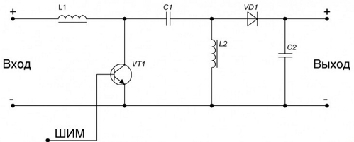
Fig. 7. Functional diagram of the SEPIC converter
It is very similar to the boost converter circuit shown in Figure 6, but has additional elements: capacitor C1 and coil L2. It is these elements that ensure the operation of the converter in the mode of undervoltage.
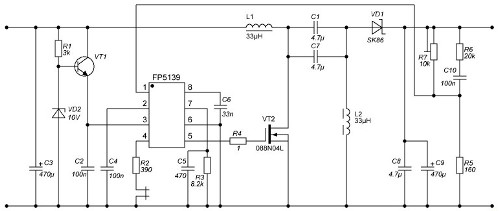
SEPIC converters are used in cases where the input voltage varies widely. An example is the 4V-35V to 1.23V-32V Boost Buck Voltage Step Up / Down Converter Regulator. It is under this name that a converter is sold in Chinese stores, the circuit of which is shown in Figure 8 (click on the picture to enlarge).
Fig. 8. Schematic diagram of the SEPIC converter
Figure 9 shows the appearance of the board with the designation of the main elements.
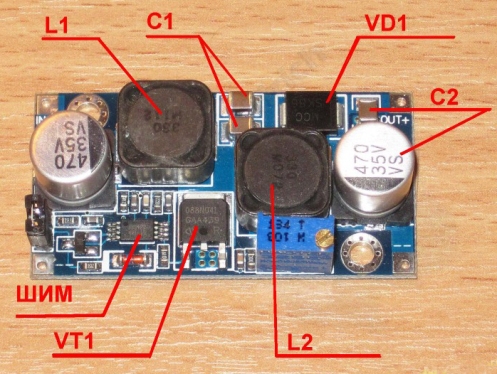
Fig. 9. Appearance of the SEPIC Converter
The figure shows the main parts in accordance with Figure 7. You should pay attention to the presence of two coils L1 L2. Based on this feature, it can be determined that this is precisely the SEPIC converter.
The input voltage of the board can be in the range of 4 ... 35V. In this case, the output voltage can be adjusted within 1.23 ... 32V. The operating frequency of the converter is 500KHz. With a small size of 50 x 25 x 12mm, the board provides power up to 25 watts. Maximum output current up to 3A.
But here a remark should be made. If the output voltage is set to 10V, then the output current cannot be higher than 2.5A (25W). With an output voltage of 5V and a maximum current of 3A, the power will be only 15W. The main thing here is not to overdo it: either do not exceed the maximum allowable power, or do not go beyond the permissible current.
See also: Switching power supplies - principle of operation
Boris Aladyshkin
See also at bgv.electricianexp.com
:

