Categories: Featured Articles » Interesting electrical news
Number of views: 31616
Comments on the article: 0
Graphene Electronics - 21st Century Miracle
 The article describes the prospects for the use of graphene and carbon nanotubes in microelectronics.
Listening to the thoughtful arguments of government officials about the need to develop nanotechnology, one involuntarily marvels at the inconsistency of their actions: funds incomparable with the budget of science are allocated for defense. Moreover, now the money invested in scientific research will allow not only to radically change people's lives, but also come close to solving the problem of human immortality.
Speaking of nanotechnology, first come to mind discovery of graphene and carbon nanotubes. It is with them that scientists associate a breakthrough in the field of electronics and pharmacology in the 21st century. The creation of quantum computers, signal reading systems at the cellular level, nanorobots for treating the body - this is just a small list of opportunities that open up. Now these opportunities have moved from the realm of fantasy to the field of laboratory development.
A special topic is microelectronics. Modern microprocessors and memory chips already overcome the value of technological standards of 10 nanometers. Ahead line 4-6 nm. But the further the developers move along the miniaturization path, the more difficult the tasks have to be solved. Engineers came close to the physical limits of silicon chips. Those who are interested in modern microprocessors know that their speed is slowed down at a clock frequency of about 4 GHz and does not increase further.
Silicon is an excellent material for microelectronics, but has a significant drawback - poor thermal conductivity. And with an increase in clock frequency and element density, this drawback becomes a barrier to the further development of microelectronics.
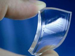
Fortunately, today there is a real opportunity to use alternative materials. it graphene, two-dimensional form of carbon and carbon nanotubeswhich are a three-dimensional crystalline form of the same carbon. The very first research results led to the creation of graphene transistorsoperating at frequencies up to 300 GHz. Moreover, the prototypes retained their characteristics at temperatures of 125 degrees Celsius.
History of the discovery of graphene miracle
 Selflessly painting the walls of rooms in early childhood with a simple pencil, we did not suspect that we were engaged in serious science - we produced graphene experiments. Thrashing from parents who did not appreciate the scientific value of experiments turned many away from science, but not all. In 2010, two Russians, an employee of the University of Manchester (Great Britain) Andrei Geim and a scientist from Chernogolovka (Russia) Konstantin Novoseltsev were awarded the Nobel Prize for the discovery of graphene, a new crystalline modification of carbon, one atomic layer thick.
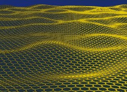
So what was the merit of scientists and the significance of the discovery? To begin with, we will deal with the very subject of discovery. Graphene is a crystalline two-dimensional surface (not a film!) One or two atomic layers thick. The most interesting thing is that theoretically graphene was “created” by theoretical physicists more than 60 years ago to describe three-dimensional carbon structures. The mathematical model of a two-dimensional lattice perfectly described the thermophysical properties of graphite and other three-dimensional carbon modifications.
But numerous attempts to create two-dimensional carbon crystals ended in failure. The “bearish” service in these searches was provided by theorists who mathematically substantiated the impossibility of the existence of crystalline surfaces. It was difficult not to believe them: after all, it was Leo Landau and Peierls - the largest theoretical physicists of the 20th century.
They made undeniable mathematical arguments that regular flat crystal structures are unstable, because due to thermal vibrations, the atoms leave the nodes of such crystals and the order is disturbed. The situation was aggravated by the fact that in real experiments, the theoretical calculations of scientists received full confirmation. The idea of synthesizing graphene was abandoned for a long time.
And only in 2004, scientists were able to obtain, and most importantly, prove that graphene is a reality. To obtain graphene, a special technique of chemical cleavage of graphite crystalline planes was used. Similar processes occur when drawing with pencil on rough surfaces, but the requirements for peeling conditions of samples are immeasurably stricter.
The second difficulty was the proof of the existence of a graphene structure. How can one observe a surface with a thickness of one atomic layer? The authors of the discovery say that if they could not find a way to observe graphene, they would not have been discovered to this day.
The ingenious technique for observing graphene was to form a two-dimensional crystalline surface on a silicon oxide substrate. And then graphene was observed under a conventional optical microscope. The correct graphene crystal lattice created an interference pattern, which was observed by the researchers.
Prospects for the practical application of graphene
 The discovery of graphene caused a reaction similar to an exploding bomb. After decades of full confidence that there is no two-dimensional modification of carbon, it suddenly turned out that with the help of fairly simple processes it can be obtained in unlimited quantities. But why?
The fact is that such a modification of carbon possesses properties that, usually restrained by scientists, give epithets fantastic, wonderful, unique. And they can be trusted. Hundreds of applications of this material are offered today, and every week appears information on new features of graphene.
Even a short list is impressive: microchips with a density of more than 10 billion field-effect transistors per square centimeter, quantum computers, sensors a few nanometers in size are only in electronics. And also rechargeable batteries of fantastic capacity, water filters that trap any impurities and much more.
The special properties of graphene allow not only to efficiently remove heat, but also to convert it back into electrical energy. Given that the graphene lattice (plane) has a thickness of one atomic layer, it is easy to predict that the density of the element on the chip will increase sharply and can reach 10 billion transistor per square centimeter. Already today implemented graphene transistors and microcircuits, frequency mixers, modulators operating at frequencies above 10 GHz.
The developers are no less optimistic about the use of carbon nanotubes in microelectronics. Based on them, transistor structures have already been implemented, and recently, IBM specialists demonstrated a microcircuit on which 10 thousand nanotubes were formed.
Of course, carbon materials cannot immediately replace silicon in microelectronics. But the creation of hybrid microcircuits, which take advantage of both materials, is already on the commercial level. Not far off is the day when microprocessors appear in a regular mobile device, the computing power of which will exceed the performance of modern supercomputers.
Do not think that all these applications are a matter of the distant future. The giants of the electronic industry - IBM, Samsung and many commercial research laboratories have joined the race for the practical implementation of scientific discovery. According to experts, in the next decade, graphene will become familiar material. And some joke that the Silicon Valley in California will have to be renamed Graphite.
See also at bgv.electricianexp.com
:
