Categories: Featured Articles » Sharing experience
Number of views: 1553
Comments on the article: 0
Export from Sprint-Layout - to Gerber format for ordering board production
In recent years, many have ordered the manufacture of printed circuit boards in China. And this is not at all surprising, because on Aliexpress alone there are a huge number of enterprises offering to manufacture at an affordable price printed circuit boards in any quantity, and even with free international delivery.
But there is one feature in this process: all PCB manufacturers require sending project files exclusively in Gerber format to them. The reason for this provision is that Gerber is a file format that is very convenient for modern equipment, which is a way of textual description of all the smallest elements of a PCB design in the form of easily reproducible commands.
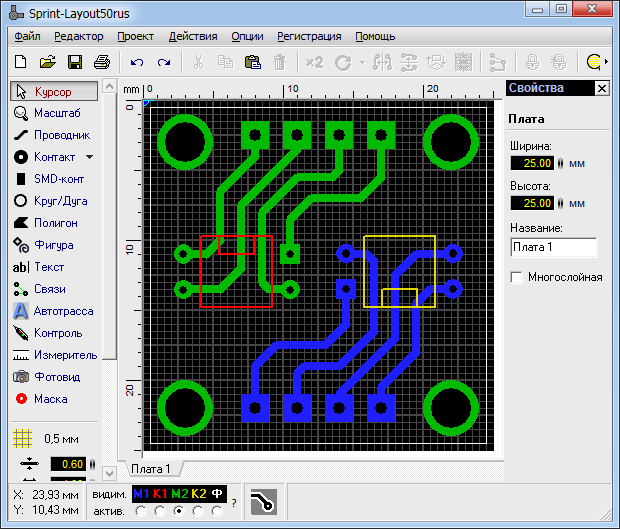
However, not everyone who is interested in the manufacture of printed circuit boards and is engaged in the development of electronics only at the amateur level, has powerful development tools that immediately give out the Gerber format. Many electronic engineers have been using SprintLayout only for wiring their boards for years, and they are quite happy with that.
The good news is that even from such a simple PCB layout program like Sprint Layout, you can export the project to a set of Gerber format files, and thanks to this feature, you can still order the production of boards in China. Let’s take a look at how to export files from Sprint Layout to Gerber format in order to be accepted.
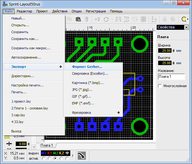
When the board is divorced, click “File”, select “Export”, then “Gerber Format”.
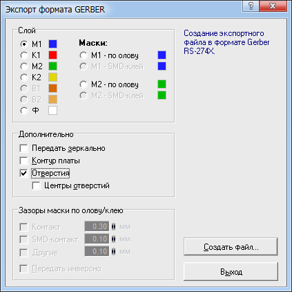
The M1 layer is the top layer of copper, in fact - tracks and soldering spots, with or without holes (for SMD components), which will be located on top. If this layer is, then put a checkmark "Holes", click "Create file ...".

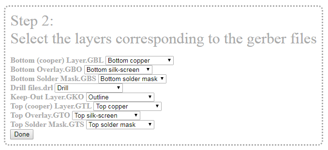
This file is saved with the same name and extension: Top (cooper) Layer.GTL
From the name it is clear that this is the top layer, that it is copper, and the file extension is individual - GTL, which is peculiar to this layer and no other.
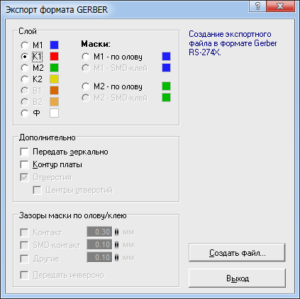
The next step is to export layer K1, if needed. This is a layer of silk-screen printing, a drawing that will be on top of the board. If the components are planned to be installed on top, then they are usually depicted with the corresponding symbols on the board for ease of subsequent installation. There may also be inscriptions and other designations.

Click "Create File ...", and save this file with the same name and extension: Top Overlay.GTO
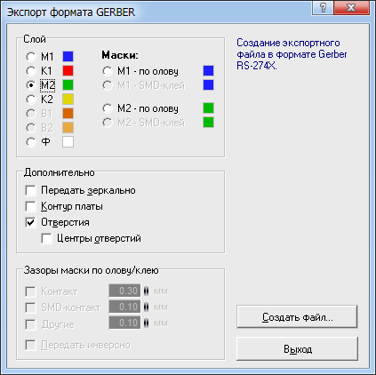
The next layer is M2. This is a layer of copper below. In fact, the tracks that will connect the output elements installed in the holes on the board from above. Put a check in the “Holes” box, click “Create File ...”.

Save the M2 layer file like this: Bottom (cooper) Layer.GBL
Again, the name, as you can see, speaks for itself.

Layer K2 - silkscreen bottom of the board. This may be a drawing of the components that will be installed on the bottom of the board, or some inscription, up to the author’s autograph.

Save the K2 layer file like this: Bottom Overlay.GBO
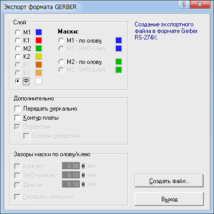
Layer F - a white line along the edge of the board, indicating its border. A very important layer on which the board will be cut on the machine.

Save the layer file F as follows: Keep-Out Layer.GKO
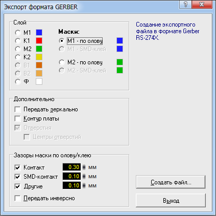
M1 mask layer - on tin. A protective mask is on top of the board, which will cover the tracks and the entire board from above, with the exception of pads. The clearances around the contacts are set in millimeters.

Save the file of the upper mask M1 as follows: Top Solder Mask.GTS
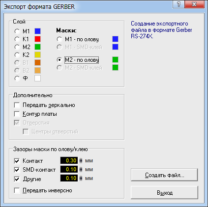
The layer of the M2 mask is tin. A protective mask is on the bottom of the board, which will cover the tracks and the entire board from below with the exception of pads. Clearances around the contacts are also set in millimeters.

Save the file of the lower M2 mask as follows: Bottom Solder Mask.GBS
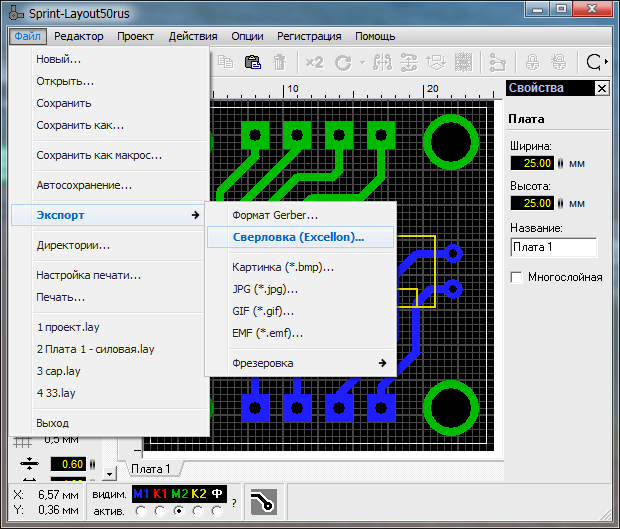
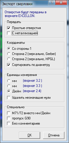
When the main layers are exported, it remains to save the file with the coordinates and diameters of the holes. Here you will find information about holes that are marked as a Contact element.
Click “File”, “Export”, “Drilling (Excellon)”, put any checkmarks you need, click “OK”.

Save the hole drilling file like this: Drill files.drl
You should get the following list of files (unnecessary ones may be missing):
-
Bottom (cooper) Layer.GBL - Lower Tracks
-
Bottom Overlay.GBO - Lower Screen Printing
-
Bottom Solder Mask.GBS - Bottom Protective Mask
-
Drill files.drl - Keep-Out Holes Layer.GKO - Board Border
-
Top (cooper) Layer.GTL - Upper Tracks
-
Top Overlay.GTO - Top Screen Printing
-
Top Solder Mask.GTS - Top Protective Mask
Before sending to production, it is advisable to check the files, see what happened. It is convenient to do this using the service.
It is enough to drag and drop files, indicate which layer means what, and click "Done".
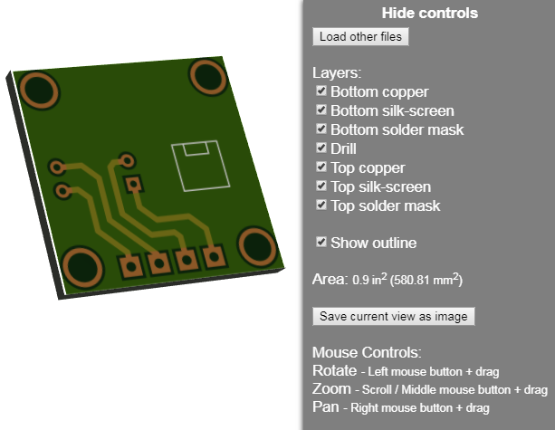
Here you can spin the board in 3D, make sure that everything is done as it should. After that, it remains to add all the files to the archive and transfer it via the Internet to the manufacturer.
See also at i.electricianexp.com
:
