Categories: Featured Articles » Interesting Facts
Number of views: 3568
Comments on the article: 0
How do LEDs
Already in 2007, in one of the reports at the Beijing Conference of the International Commission on Lighting, the importance of economy and environmental friendliness of both already used and still being developed, more advanced lighting products was emphasized.
The primary accent was made by the speakers on a more rational and efficient use of light. And this was not at all a call to somehow reduce the illumination. As one of the most important steps towards this goal, the development and implementation of energetically more efficient and environmentally friendly light sources is highlighted - LEDs.

High tech industry
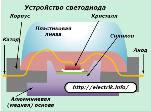
LEDs are semiconductor electrical products designed to receive light due to the electric current passing through the pn junction. But not every pn junction emits light.
In order to receive light from a semiconductor, certain conditions must be met: the forbidden transition zone on the semiconductor must be so wide that the energy of the resulting quanta is close to the energy of the visible light quanta, and the probability of radiation in the process of recombination of electron-hole pairs should be high.
To comply with these conditions, the fabricated crystal should have a minimum of defects leading to the recombination of electrons with holes without radiation. This is not easy to achieve, just a p-n junction will not be enough, you have to create multilayer semiconductor structures - heterostructures, which, incidentally, laid the foundation for a new stage in the development of the technology of production of light-emitting diodes.
The creation of LEDs is fraught with certain obstacles, because this lighting industry is constantly evolving, and there are still no certain established regulations in it.
The production process of LEDs, as well as methods for their direct operation, are still not subject to some general documents, so each major manufacturer develops its own principles for selecting the appropriate products.
There are no international agreements. And even though some very positive results have already been achieved in recent years, there are still no unified requirements for led technology. And now you will understand everything, as we will further examine the LED production technology step by step.
Crystal formation
Crystal LED is grown. The key process in this entire chain is called organometallic epitaxy, in which oriented epitaxial crystal growth is realized on the substrate.
The semiconductor is grown by thermal pyrolysis (decomposition) of organometallic compounds that contain the necessary chemical elements. Here, the presence of pure gases is mandatory, the presence of which is ensured by modern installations.
The grown layer must have a certain thickness, which is controlled during the epitaxy process. In this case, the structure on the surface of the substrate should be homogeneous.
Reliable and high-quality installations for epitaxial growth are very expensive, and the process of obtaining high-quality materials for the production of high-quality LEDs has been going on for more than one year.

Chip making
To obtain a chip, a crystal grown on a substrate is subjected to etching, then contacts are created and the resulting sample is cut into pieces. This is called "planar film processing." One whole film is cut into thousands of small chips.
Chip sorting
Sorting chopped chips is called binning. Beans are groups. Sorting is very important, but it is often forgotten, analyzing the process of creating LEDs.
The bottom line is that in any production it is important to select high-quality products, as well as sort the product according to parameters, according to certain criteria, which is especially important for LEDs. At the stages of epitaxy, and after cutting, it is impossible to obtain thousands of crystals (chips) that are absolutely identical in characteristics.
One way or another, their characteristics will vary, and will appear in some fairly wide range of parameters. That is why the chips must be sorted by characteristics into groups (bins), so that in each group there are chips with a certain value of some parameter, suitable for the requirements of the range of a particular group: by wavelength, by voltage, by luminous flux, etc. .
As a result of binning, the LEDs will be divided by application and even by name. Some will go for some goals, others for others. The circle of consumers of the product will expand.
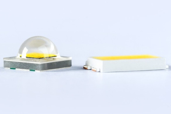
Almost finished LED
A ready-made LED is obtained at the final stage of the technological chain. Here the body of the future light source is created, the conclusions are soldered, a suitable phosphor is selected. The optical system, shape and parameters of the lens are selected.
Lenses are made of various materials (epoxy resin, plastic, silicone). Depending on the requirements, the material of the optical system is chosen. The requirements are very broad, because it is the optical system that will play a decisive role in how the light flux will be directed, what the solid angle will be, etc.
Lens Features
Lenses should be as transparent as possible, transmit light in the entire visible range. In this case, the lens should adhere well to the material of the printed circuit board, be thermostable throughout the entire service life. This means that the lens should not be affected by the radiation of the crystal and the chemical effects of the phosphor, if used.
The production process of LEDs at the OPTOGAN factory:
LEDs
LEDs are not in vain considered the best light sources. They are characterized by low power consumption, the absence of harmful components such as mercury, a safe supply voltage, high reliability, compactness and other useful qualities.
It is LEDs that allow you to build lighting systems and lighting fixtures of various shapes and sizes, with high quality: floodlights, LED strips, lamps, lamps, panels, etc.
One thing is undeniable - the LED direction in the lighting industry is developing dynamically throughout the world. Technology is the subject of attention of highly skilled specialists and scientists from many countries. In the near future, even more impressive indicators will definitely be achieved.
See also on this topic:
See also at bgv.electricianexp.com
: