Categories: How does it work
Number of views: 6484
Comments on the article: 2
How do integrated circuits
The advent of integrated circuits has made a real technological revolution in the electronics and IT industry. It would seem that only a few decades ago, for simple electronic calculations, huge tube computers were used, occupying several rooms and even entire buildings.
These computers contained many thousands of electronic lamps, which required colossal electric powers and special cooling systems for their work. Today, they are replaced by computers on integrated circuits.

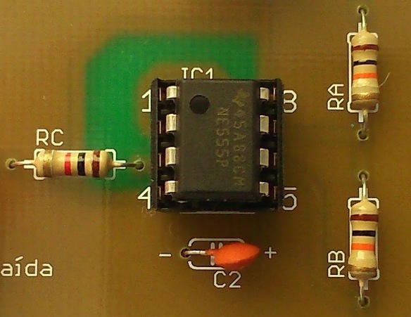
In fact, an integrated circuit is an assembly of many microscopic-sized semiconductor components placed on a substrate and packed in a miniature case.

One modern chip the size of a human nail can contain several million diodes, transistors, resistors, connecting conductors and other components inside, which in the old days would require the space of a rather large hangar for their placement.
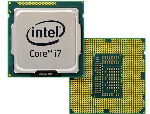
You don’t have to go far for examples, the i7 processor, for example, contains over three billion transistors on an area of less than 3 square centimeters! And this is not the limit.

Next, we will consider the basis of the process of creating chips. The microcircuit is formed according to planar (surface) technology by lithography. This means that it is, as it were, grown from a semiconductor on a silicon substrate.

The first step is to prepare a thin silicon wafer, which is obtained from a silicon single crystal by cutting from a cylindrical workpiece using a diamond-coated disk. The plate is polished under special conditions to avoid contamination and any dust.
After that, the plate is oxidized - it is exposed to oxygen at a temperature of about 1000 ° C in order to obtain on its surface a layer of a strong dielectric film of silicon dioxide with a thickness of the required number of microns. The thickness of the oxide layer thus obtained depends on the time of exposure to oxygen, as well as on the temperature of the substrate during oxidation.

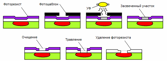
Next, a photoresist is applied to the silicon dioxide layer - a photosensitive composition, which, after irradiation, dissolves in a specific chemical substance. A stencil is placed on the photoresist - a photomask with transparent and opaque areas. Then a plate with a photoresist applied to it is exposed — it is illuminated with a source of ultraviolet radiation.
As a result of exposure, that part of the photoresist that was under the transparent areas of the photomask changes its chemical properties, and can now be easily removed along with the silicon dioxide under it with special chemicals, using plasma or another method - this is called etching. At the end of the etching, the unprotected (illuminated) places of the wafer are cleaned of the exposed photoresist and then of silicon dioxide.

After etching and purification from the non-illuminated photoresist of those parts of the substrate on which silicon dioxide remained, they begin epitaxy - they apply layers of the desired substance one atom thick onto the silicon wafer. Such layers can be applied as much as necessary. Next, the plate is heated and diffusion of ions of certain substances is carried out to obtain p and n-regions. Boron is used as an acceptor, and arsenic and phosphorus are used as donors.

At the end of the process, metallization is performed with aluminum, nickel or gold to obtain thin conductive films that will act as connecting conductors for transistors, diodes, resistors grown on the substrate in the previous stages, etc.In the same way, pads for mounting the microcircuit on the printed circuit board are output.
See also: Legendary Analog Chips
See also at bgv.electricianexp.com
:
